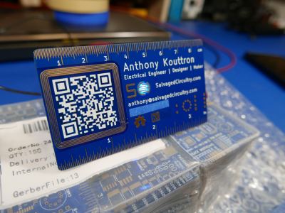

PCB Business Card
I had a very simple business card for years, but I was just plain tired of it. It was too bland and looked like all of the other business cards that I had amassed over the years. I was catching up on the Amp Hour podcast and in one of the episodes Dave Jones mentioned something that really caught my attention: bring your projects to social events. I thought about it for a bit but could not think of any good way of bringing large, partially completed projects or populated boards to an event without looking like the ultimate king-of-the-nerds. Of course, I mulled about the idea some more and thought: would it even fit in my pocket? What dimensions make it too big for a pocket? I could reduce z-height. What about cargo pants? They have bigger pockets. I could bring a jacket, but wouldn't it be odd to keep reaching for something in a jacket pocket?
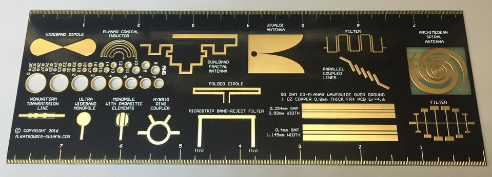
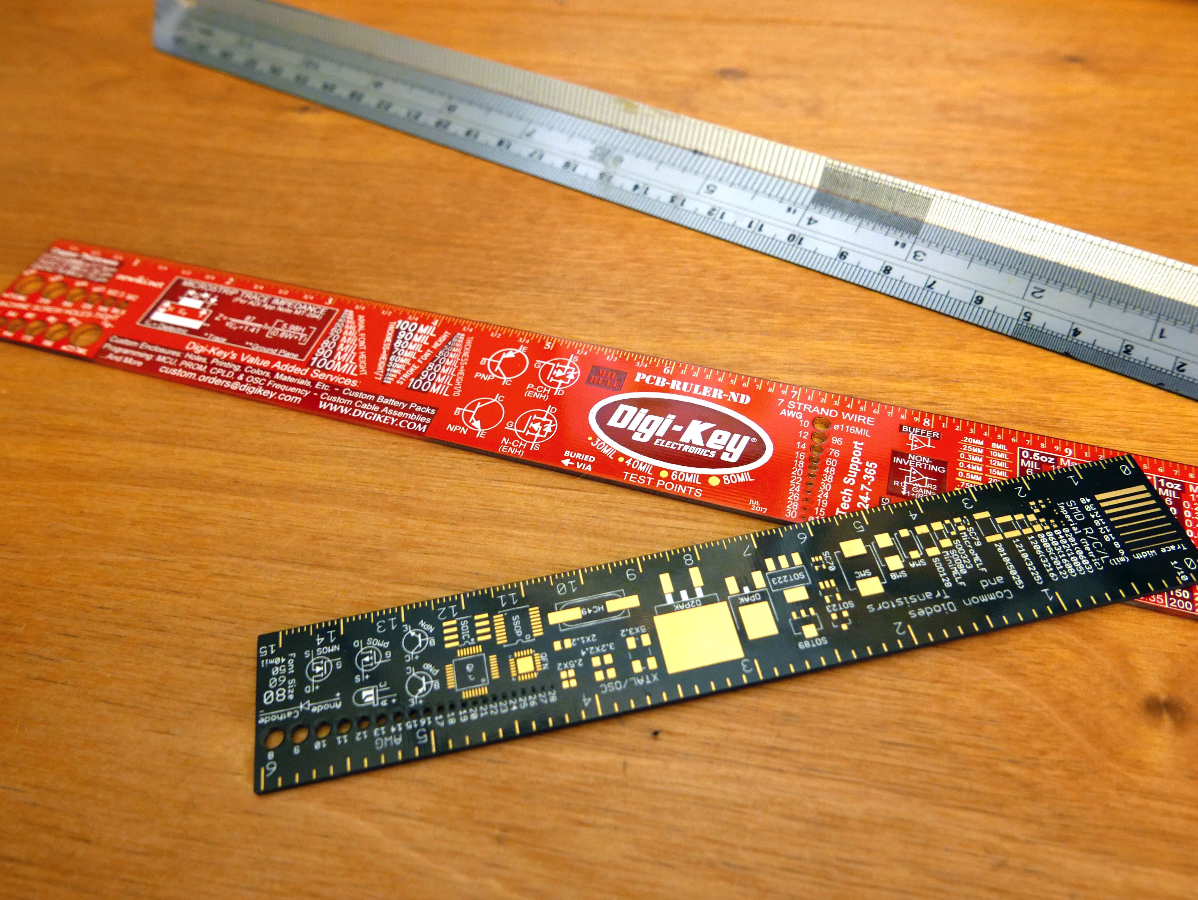
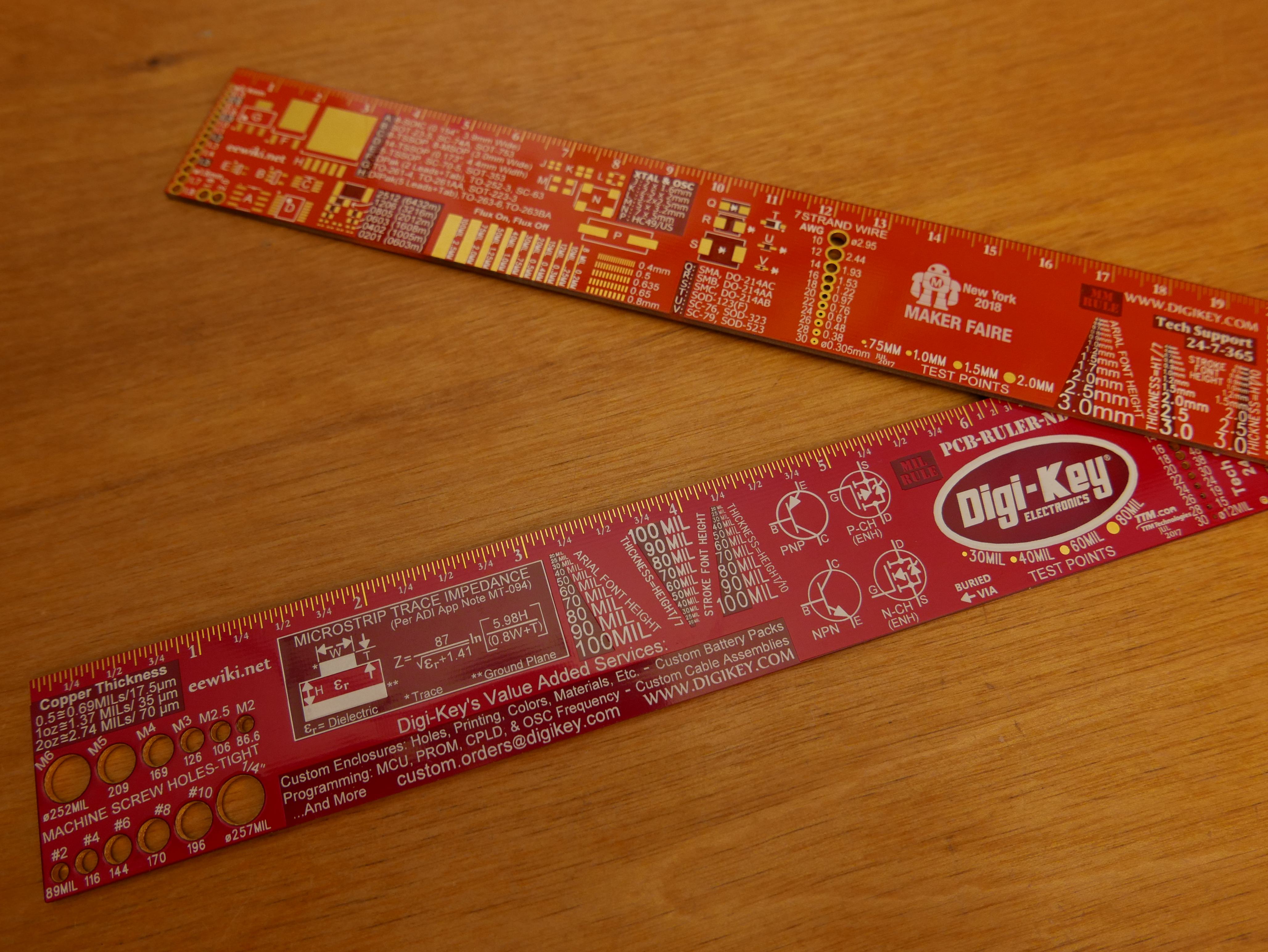
After exhausting that line of thinking, I abandoned the idea completely and continued on with my projects. I decided that I would just bring photos along to hardware meetups instead. That all changed when I discovered the "elegant PCB artwork ruler" and "RF & MW Elegant PCB ruler" designed by Makis Katsouris. I originally found them through ebay, but Makis' website, SV1AFN.com, details all aspects of the rulers along with some really top notch RF projects. Oh boy, I used "notch" as a way to describe RF projects. The jokes only get better from here folks :D.
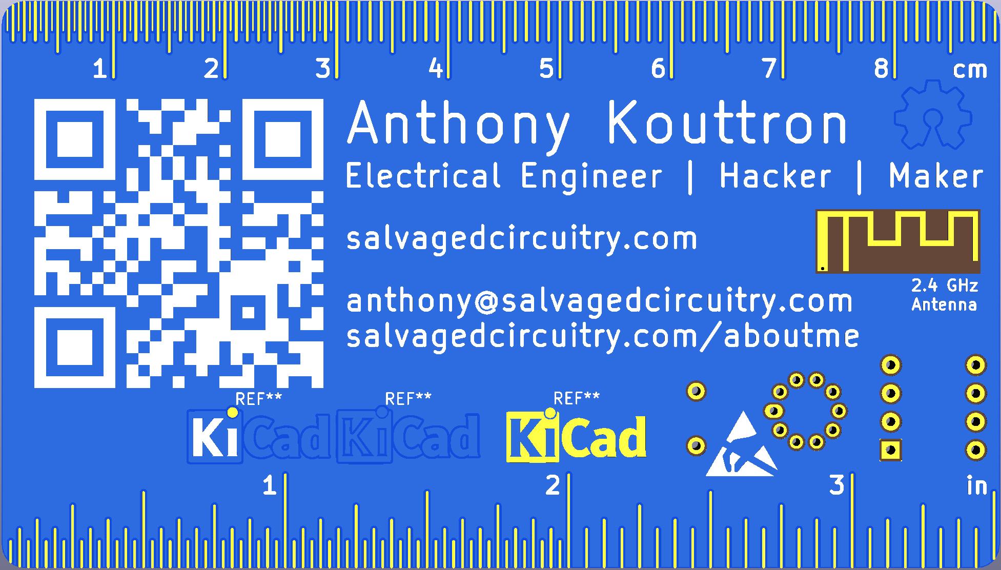
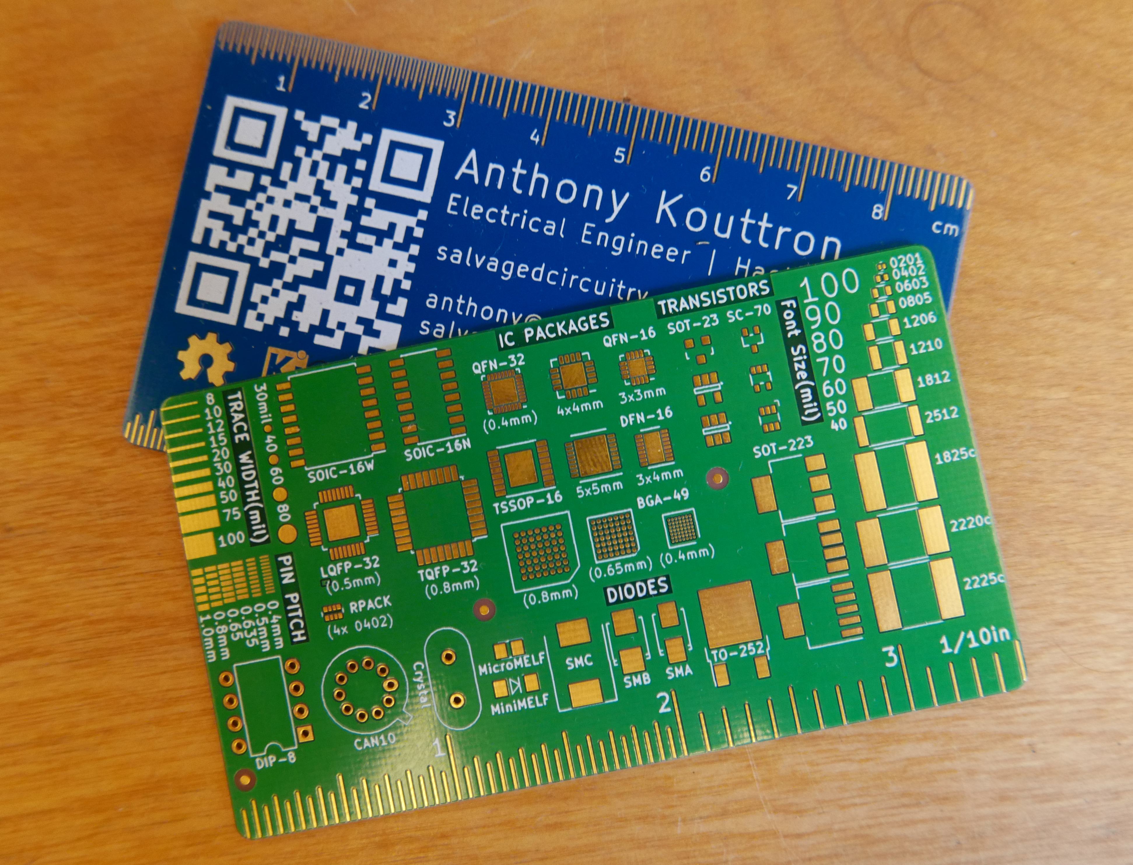
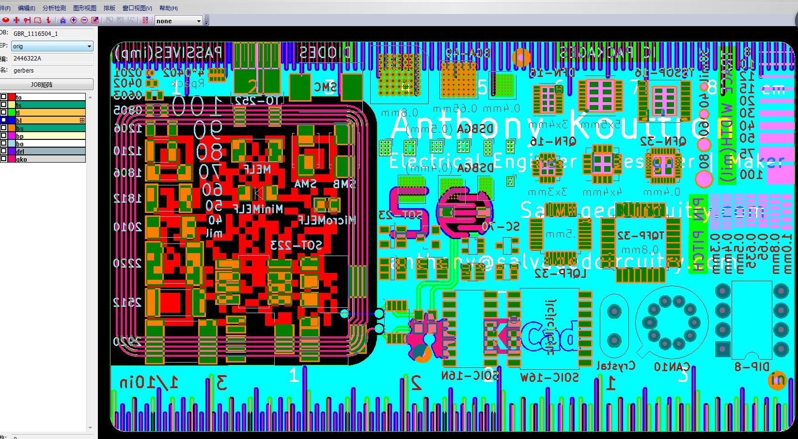
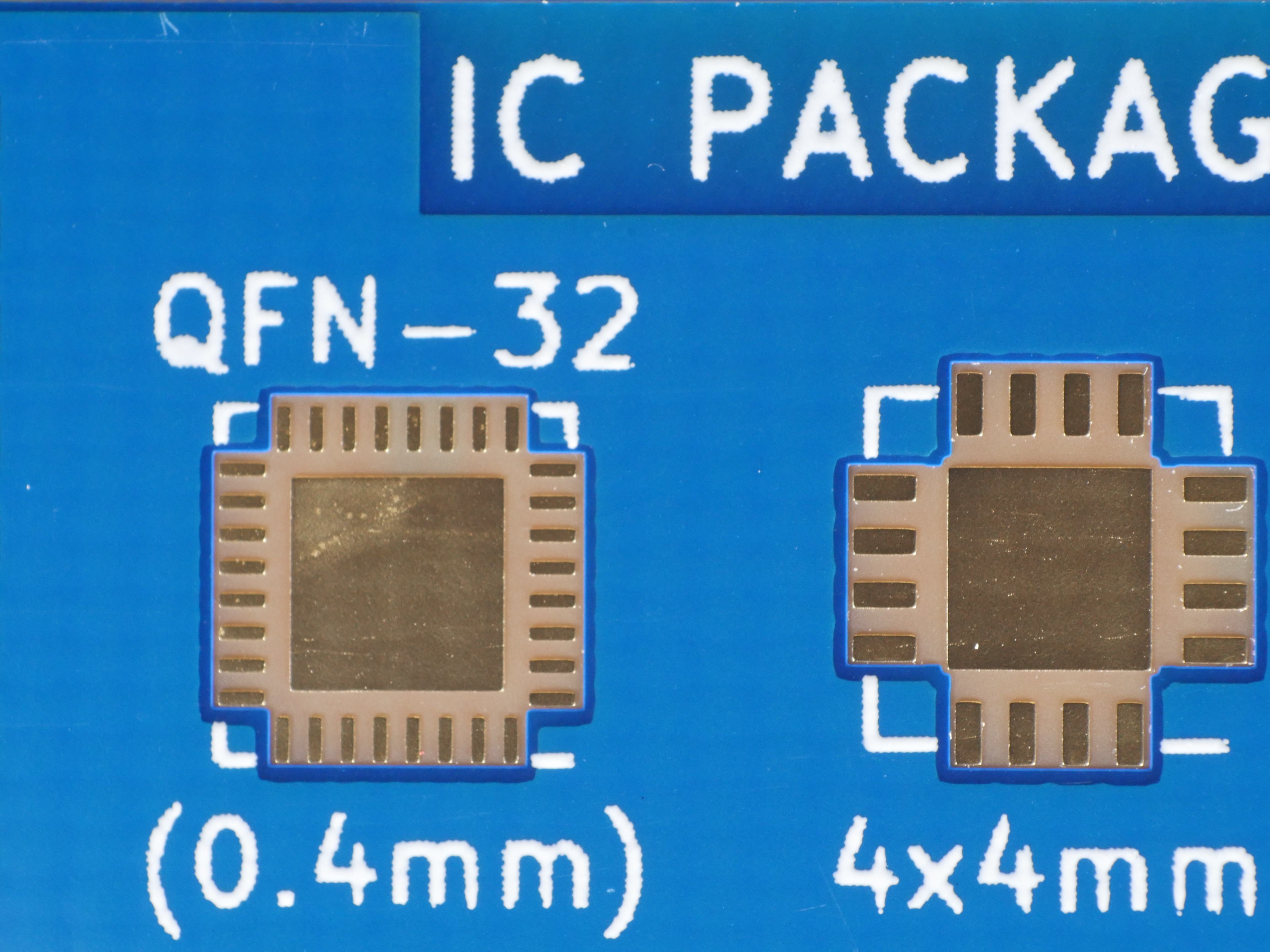
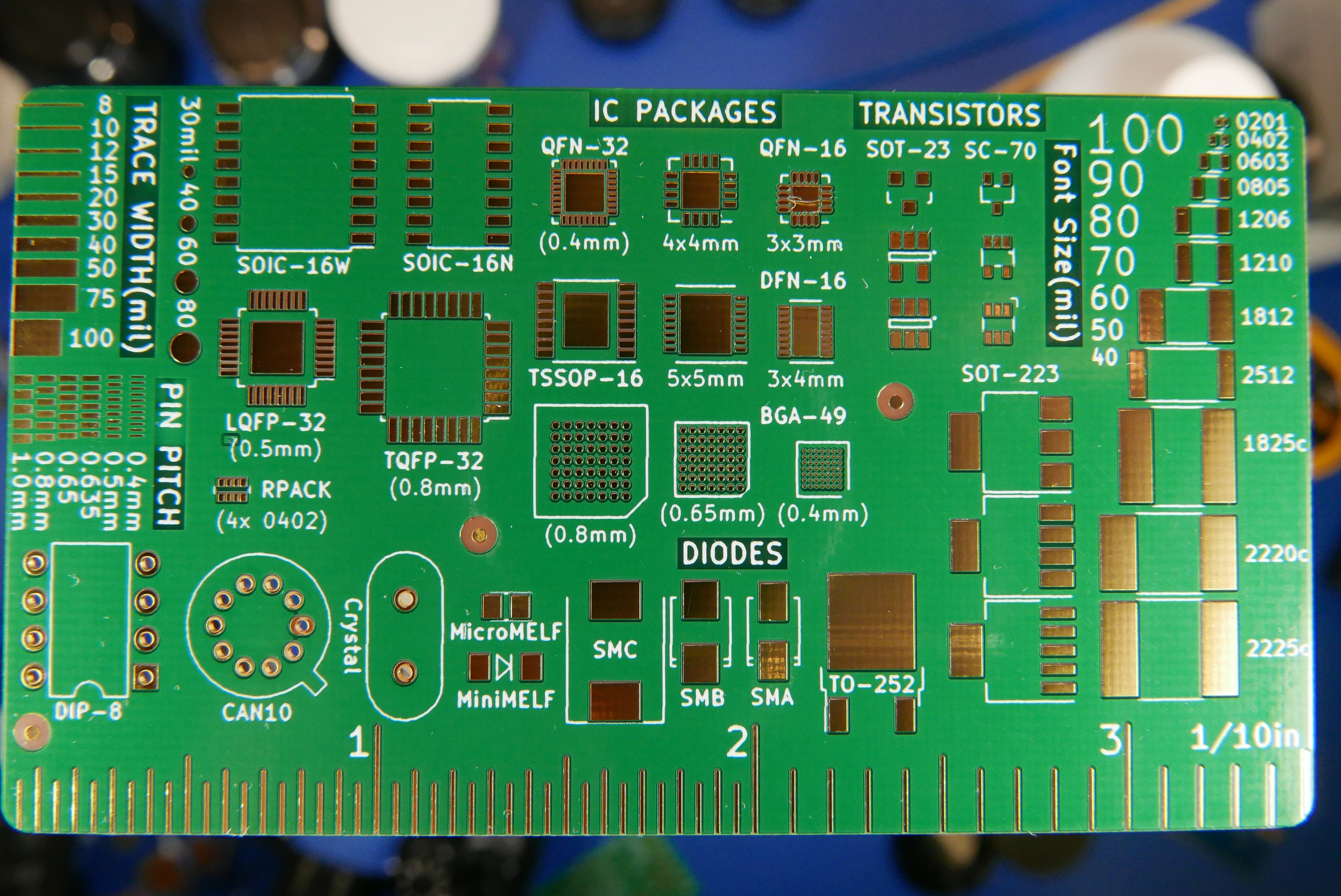
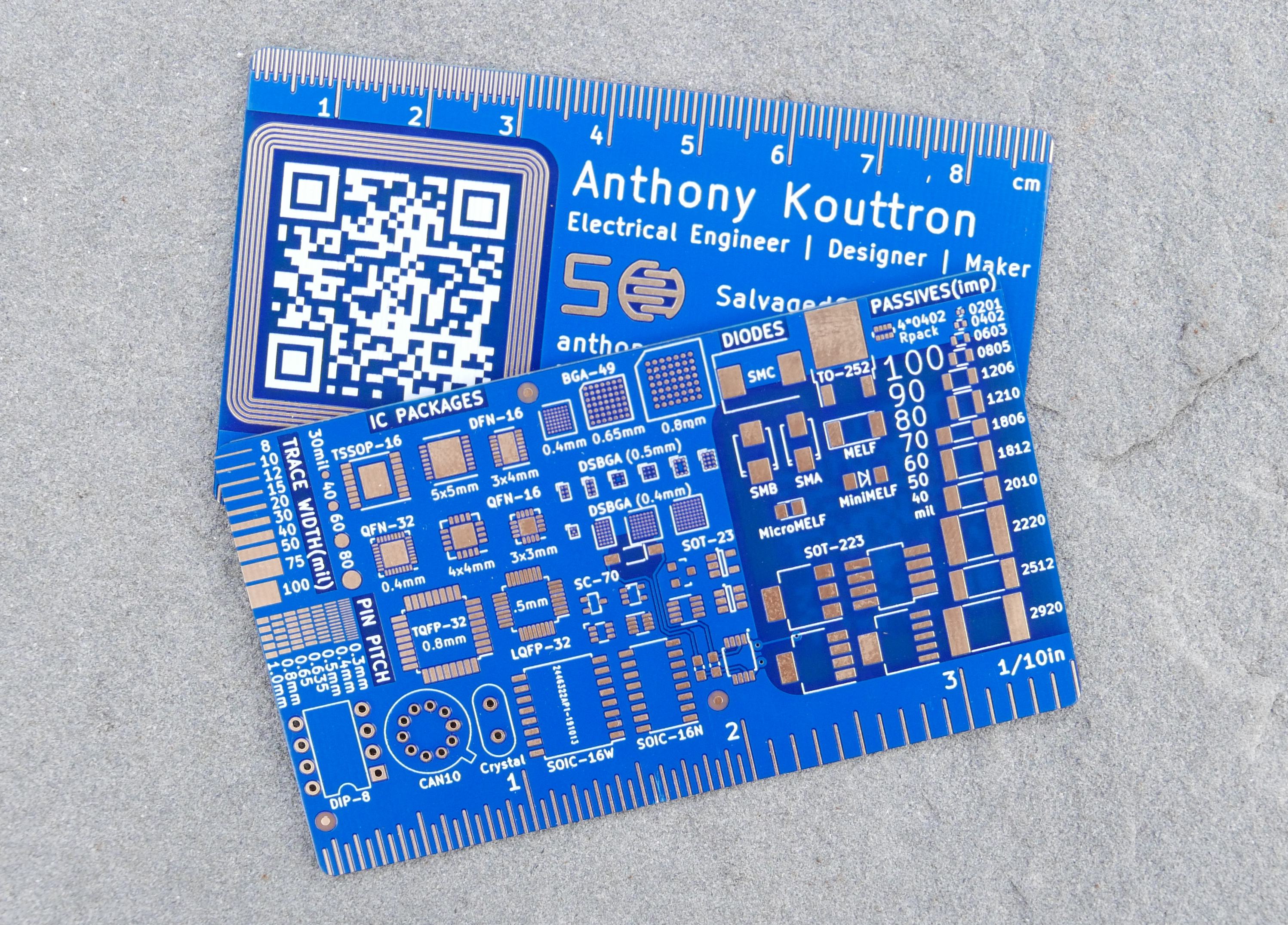
Taking inspiration from these elegant rulers along with the Sparkfun, Adafruit, Digi-Key and Nvidia rulers, I decided to morph a PCB ruler into a business card. I wanted to focus my business card design on footprints, common measurements and useful reference materials to help folks who are interested in making their own PCBs. Of course, I could fill the card with references to all the types of op-amp configurations, diode types, and trace current capacity calculations, but I wanted to make something that would put a physical size to common part package sizes instead. This way, the designer would have something tangible in front of them to gauge the actual size of a package on a board and give them a better idea of how much clearance a package would need in relation to other components on a PCB.
Sometimes the best way to start a project is to check if someone else already did the same thing. Sure, I knew that it was unlikely that I would find a business card design to my exact tastes, but I wanted to at least check if something came close. Looking at other designs on the web gave me further motivation and validation that this was indeed a great idea. My hour of searching for PCB business cards on Hackaday and Github was quite rewarding. Just look at the Business card made by Tim Jacobs. What a fantastic idea of integrating a simple MIDI device into a business card. Very neat.

Design Decisions
I settled on this very useful and succient business card made by Brian D. Carlton to use as a template. After all, I'm a KiCAD user and even if I decided to start over, the Edgecut dimensions should be the right size :D. I really liked the simplicity of Brian's heavily layout-based business card, so I took the same principle and applied it to my card. Cheers Brian on the great business card!
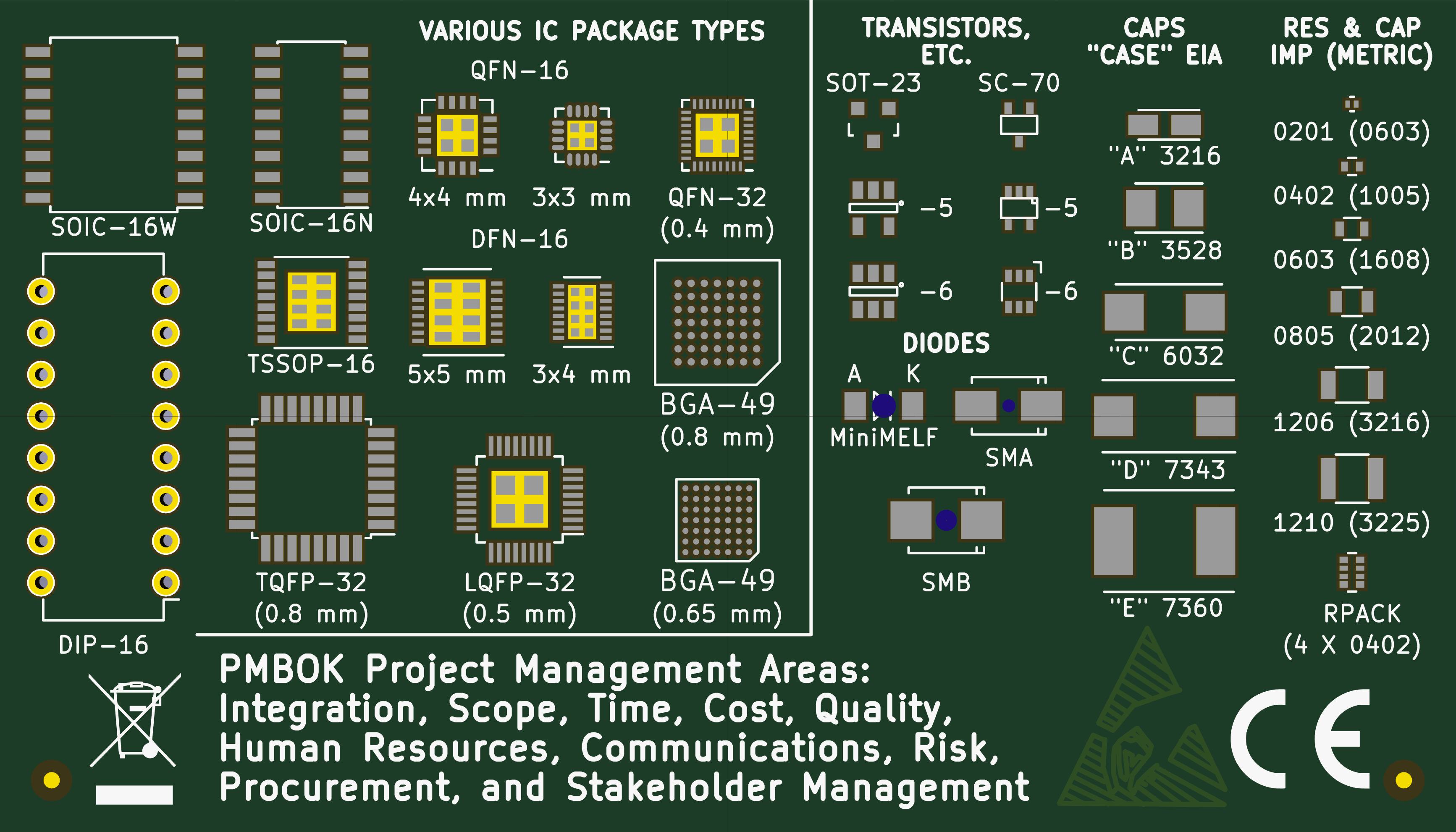
One of the first changes I made to the card was add more components. I really liked where Brian's business card was going but there was too much empty space for my tastes and I could use that space to fit in more footprints. I decided to keep a good chunk of the IC packages and transistors, but I expanded on the passive footprints, diodes and SOT packages. Here's an early iteration of my board. It's not pretty, but it's getting somewhere.
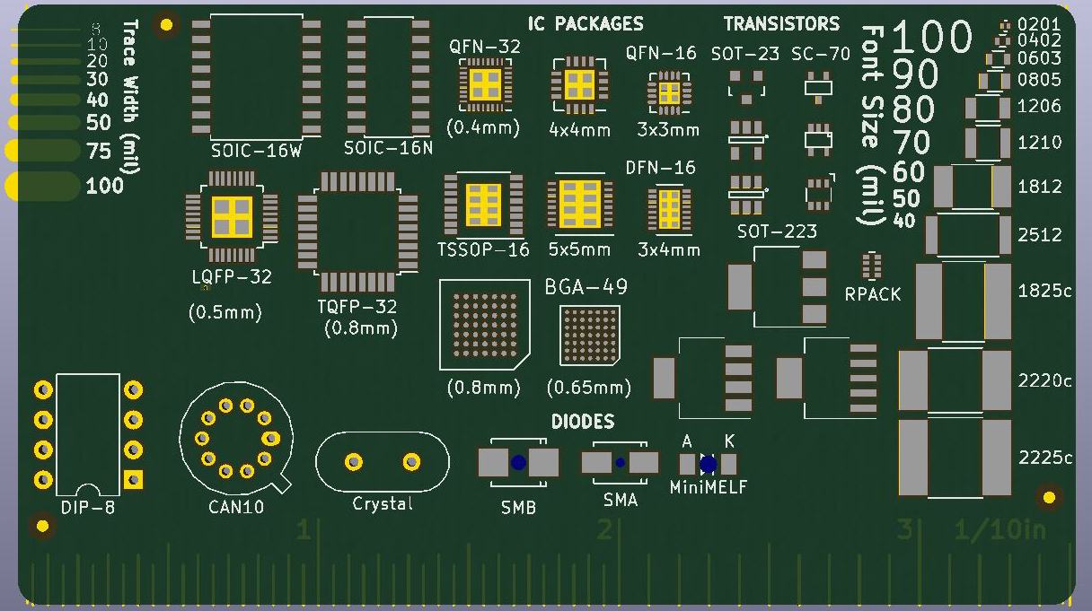
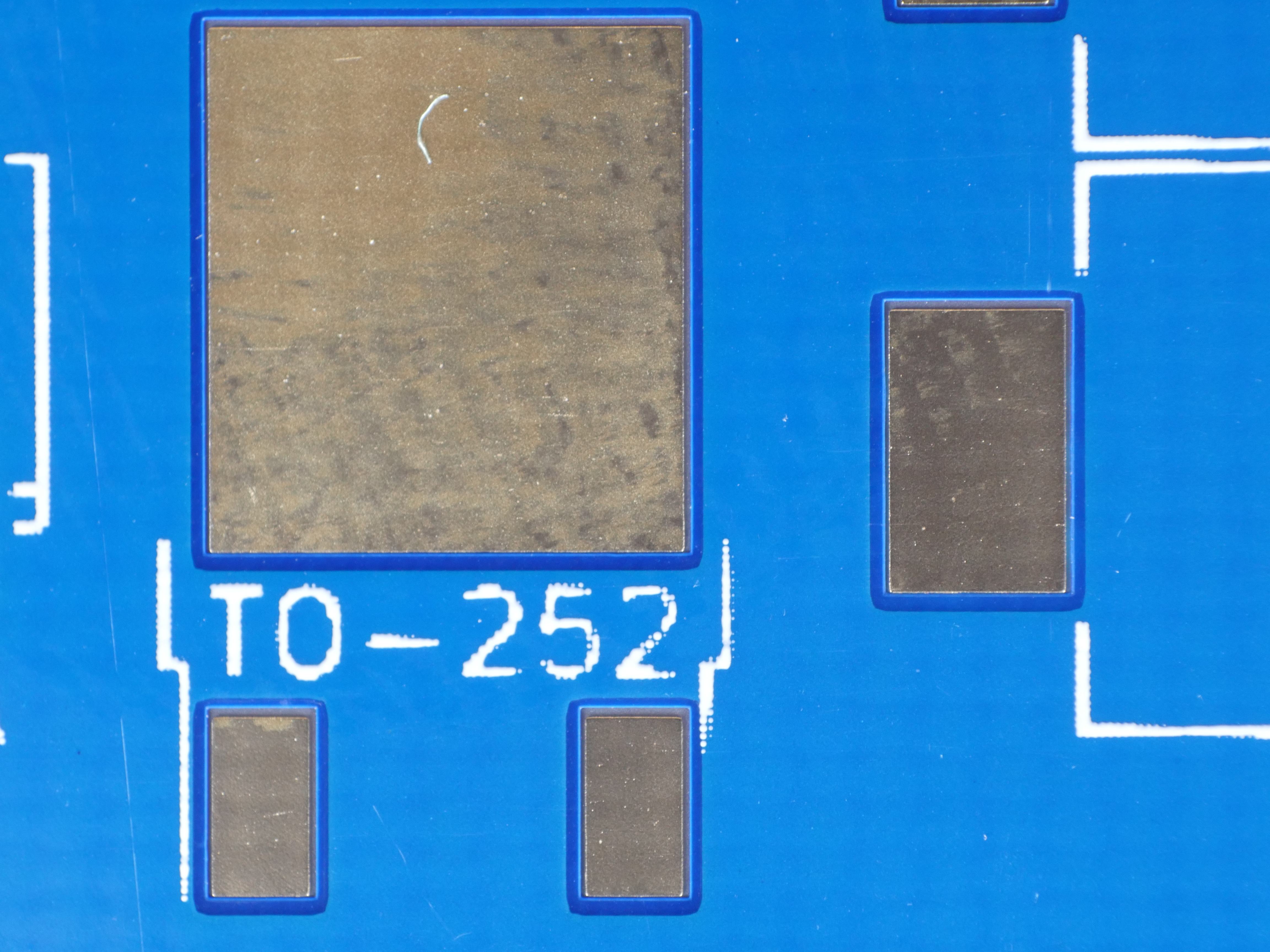
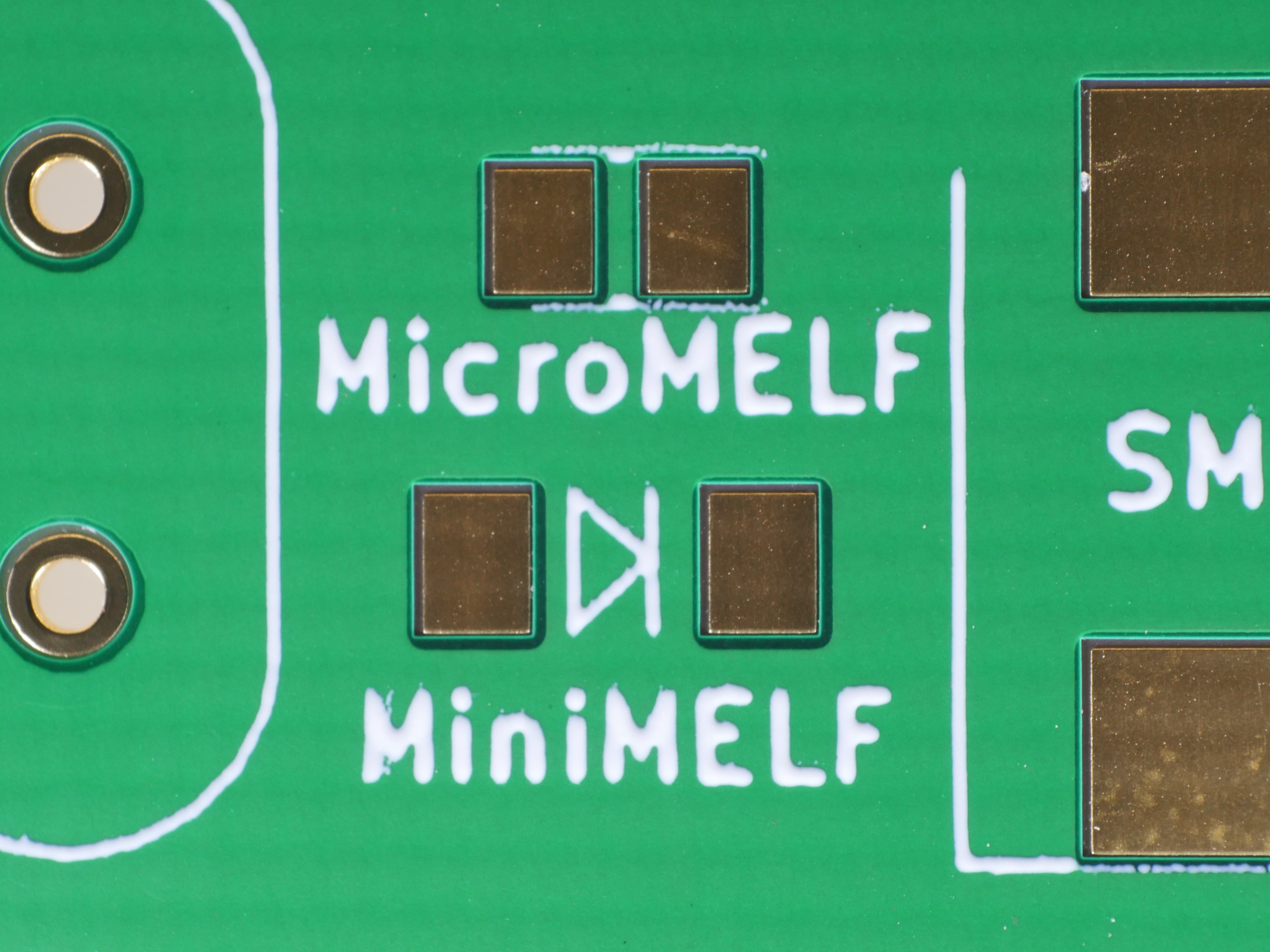
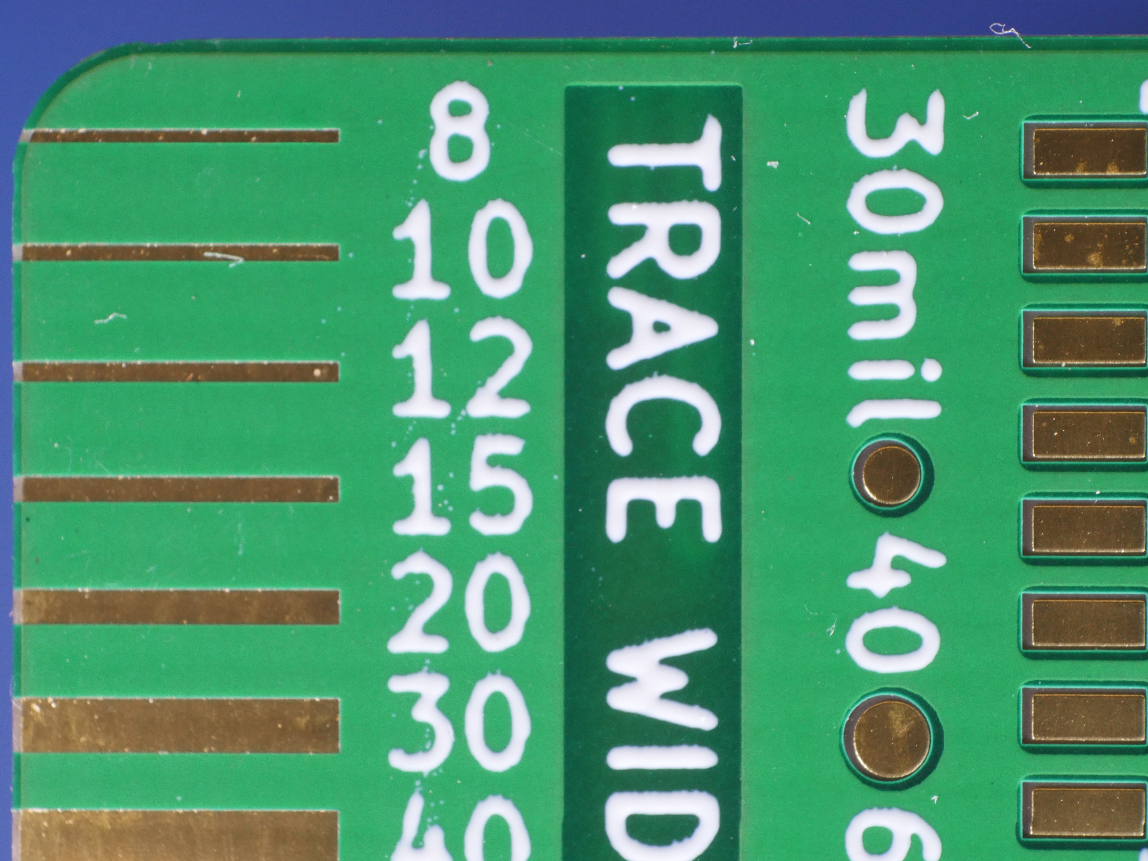
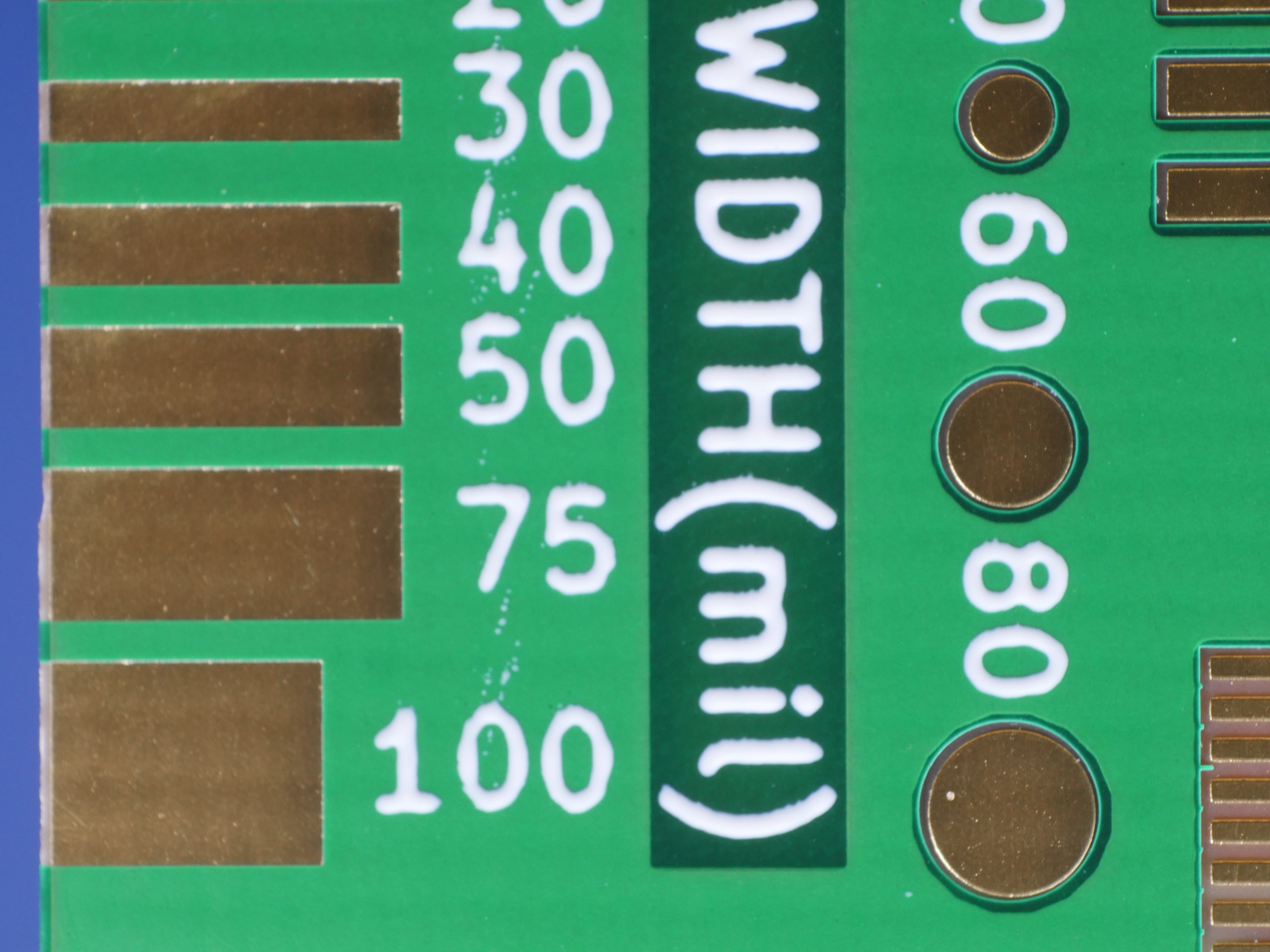
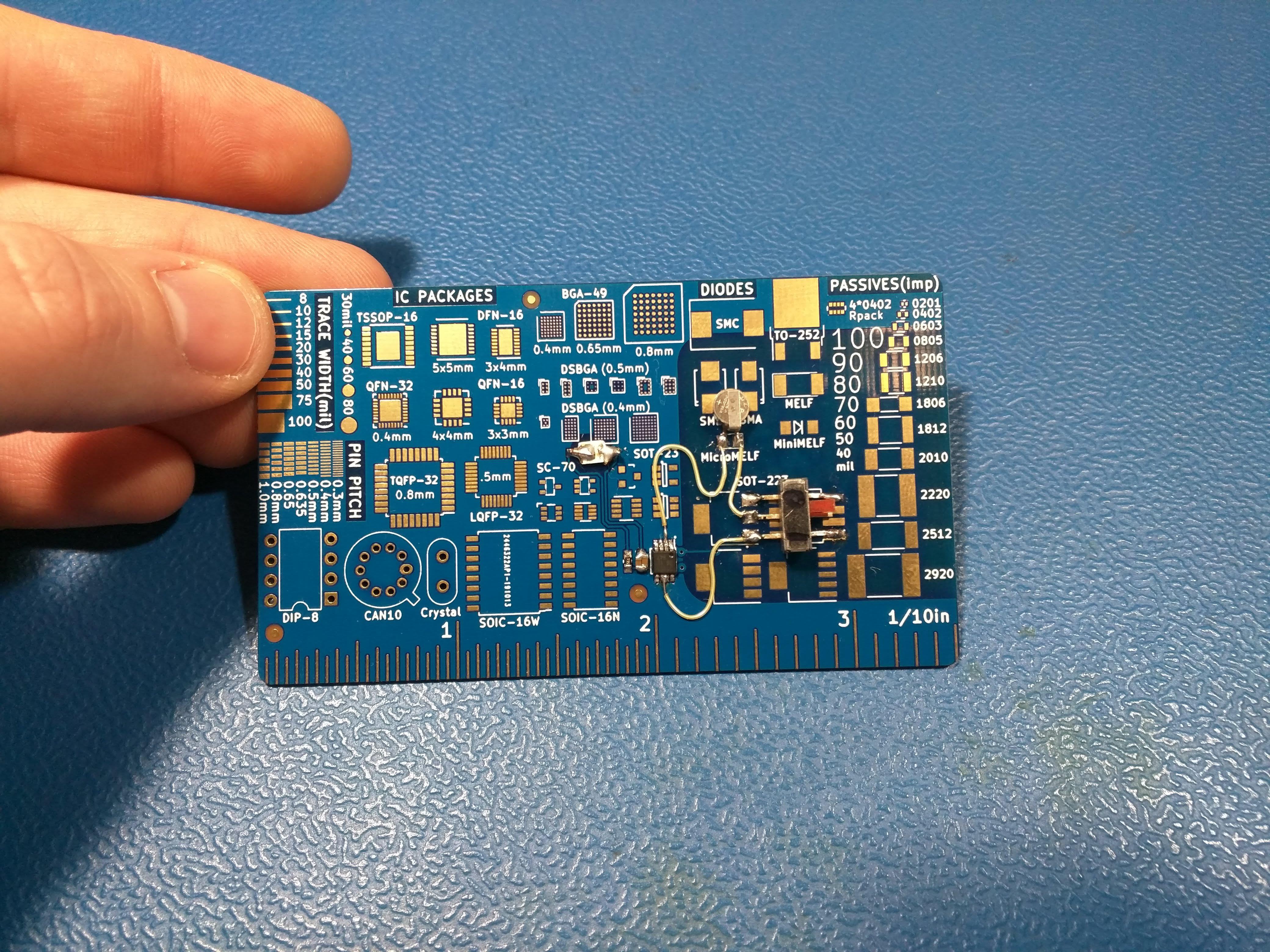
My goal was to squeeze the most out of a compact layout. I added a simple font size scale and trace width scale. I added common test pad sizes as a reference to test jig design or bed of nails testing. I added some fiducials for good practice and attached a 2.4ghz antenna, which is now even more common from the IOT craze. I didn't want to leave out common footprints from older equipment, so the TO-5 CAN10, DIP and crystal packages were added. I decided not to include hole sizing because wire strippers with included AWG sizes are pretty commonplace. Also, additional drilling adds to manufacturing time, and through-hole plating varies by pcb vendor, so it's best to skip it completely.
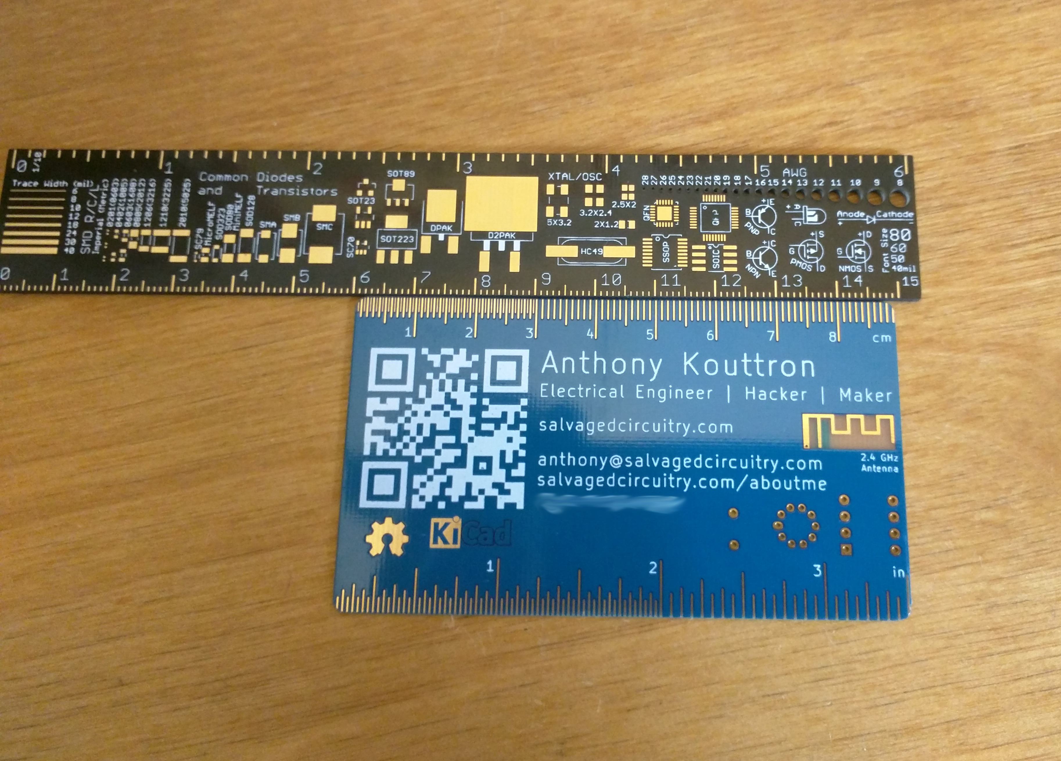
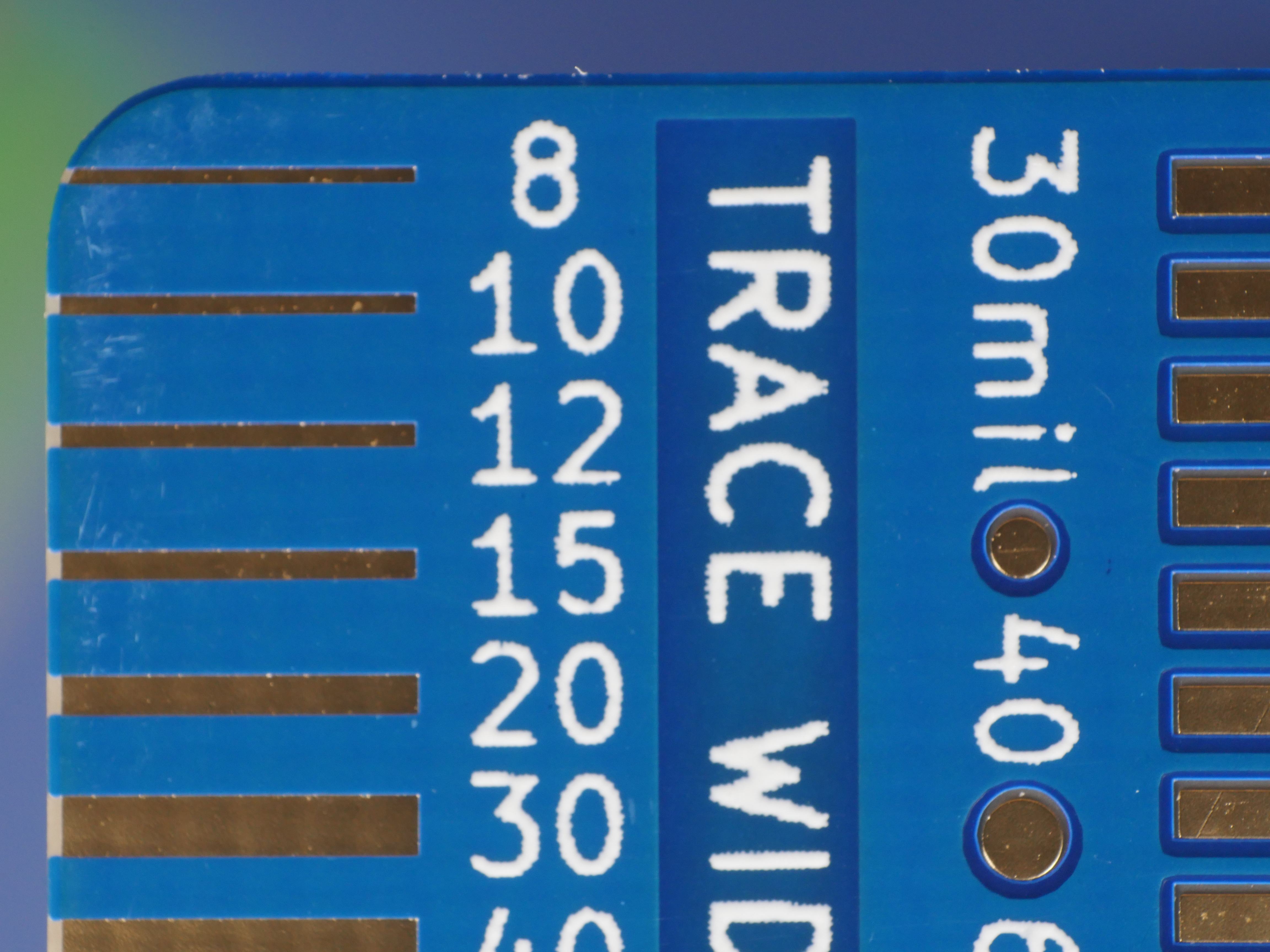
One of the biggest departures of my design is the included rulers. I designed each of the three rulers as a custom array of lines so I could mix 1/16 and 1/32 of an inch on one ruler, tenth of an inch and 5 hundredth (50 thousandths) on another and millimeters and half millimeters on another ruler. None of these types of rulers are available with the included kicad footprint library rulers. I didn't even know the KiCad library contained ruler footprints until I checked out Jan Böhmer's PCB ruler. A ruler is the last thing you'd expect in a footprint library!
The QR code was created by a qr code generator website and then converted over to a kicad mod file using the "Bitmap to Component Converter" built into Kicad. Make sure you use a high resolution image when using this tool and adjust the "Black / White threshold" slider to fine tune the "Black&white" picture preview. This picture preview is exactly how the kicad_mod file will look. I previously used the super useful Wayne & Layne img2mod Image Converter for Kicad web tool. This is a great little tool for converting images to kicad_mod files, but the one downside is that is creates huge kicad_mod files which bogs down Kicad. This is largely because it integrates the area of an image with tiny unconnected polygons instead of just creating large contiguous polygons like "Bitmap to Component Converter."
One thing to note, inverted QR codes are not always read by every barcode scanner application. I have found that lightening QR is one of the few barcode scanning apps on the android app store that works well with the inverted PCB bar code. It is a bit spammy with ads, which I'm not a fan of, but I have not found an opensource alternative yet. Apple devices with a qr code scanner built in seem to pick it up just fine.
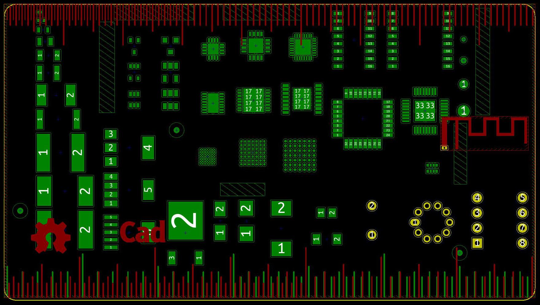
A big time sink with projects like this is ironically, layout. But not in terms of connecting everything together. Anyone can throw a footprint somewhere on a copper layer, but if you are trying to make a legible reference card, equivalent spacing becomes paramount. Ideally, you don't want some footprint references to be harder to read than others and you certainly don't want silkscreen overlap, causing the user to think two references are one! Footprint overlap is also a big no-no.
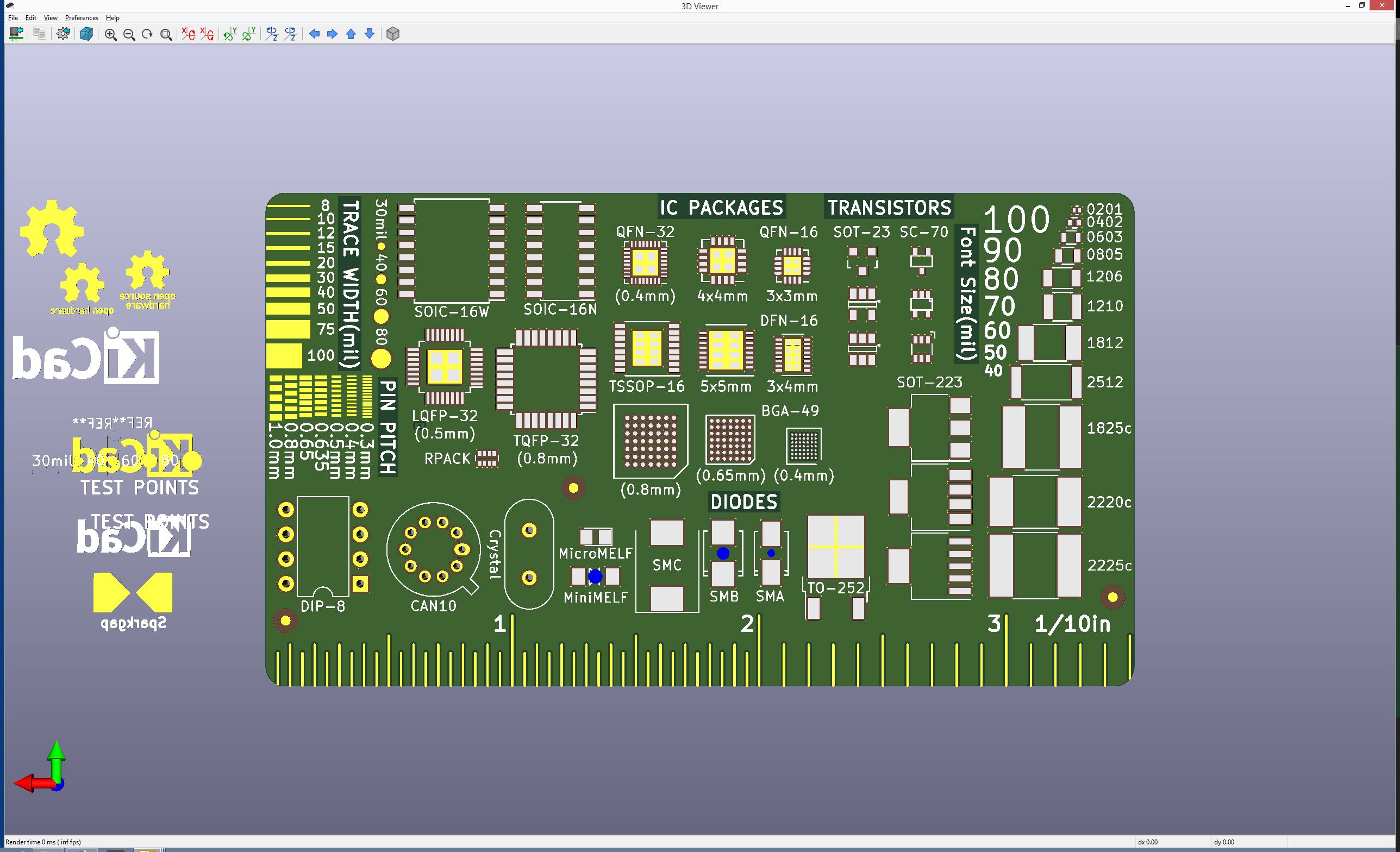
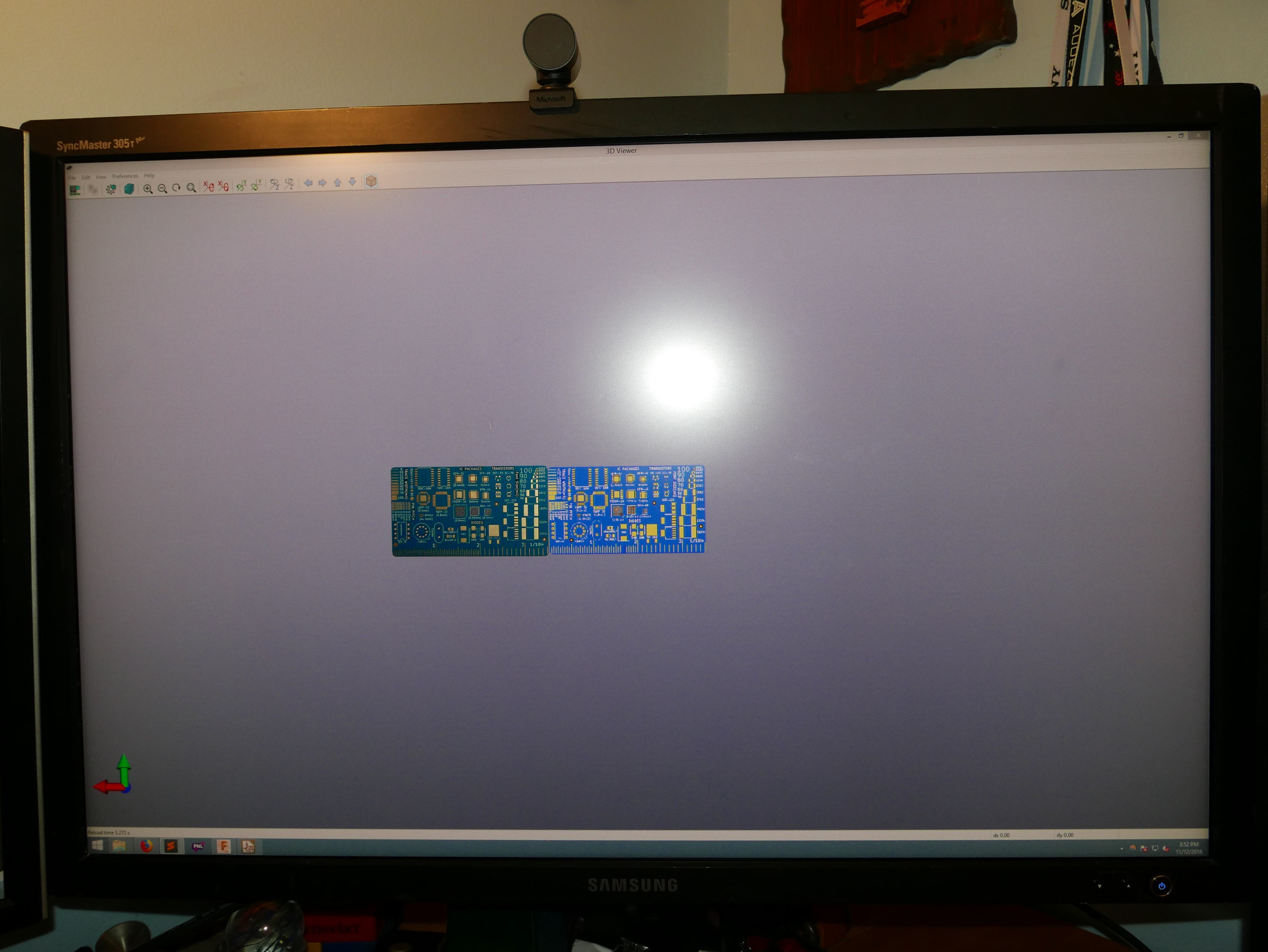
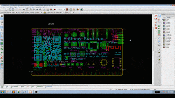
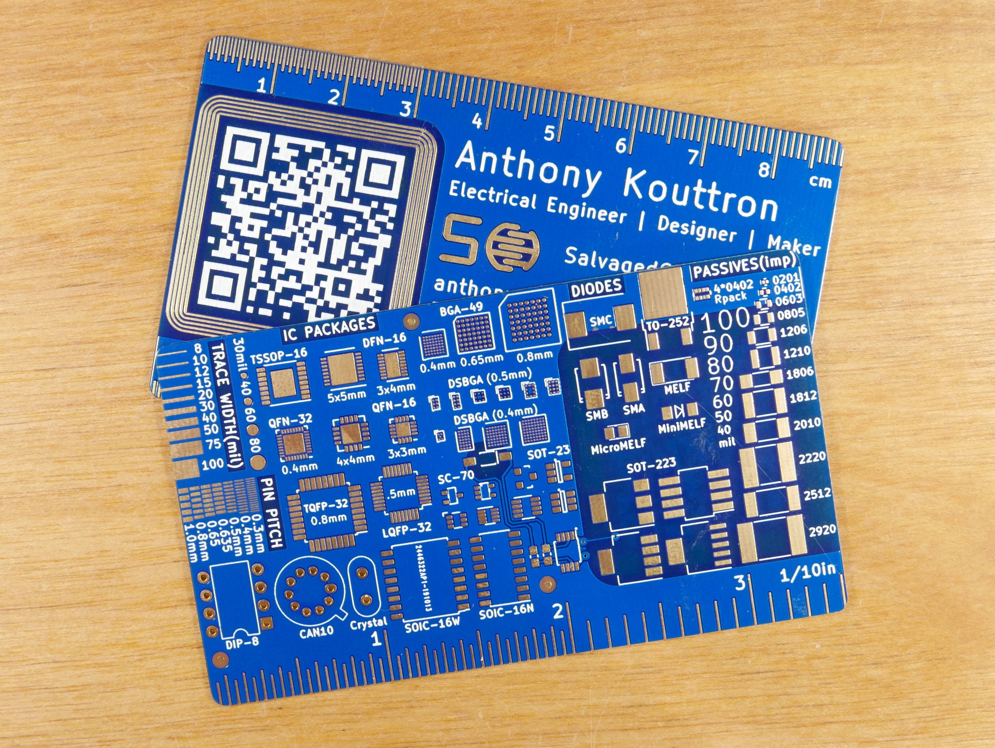
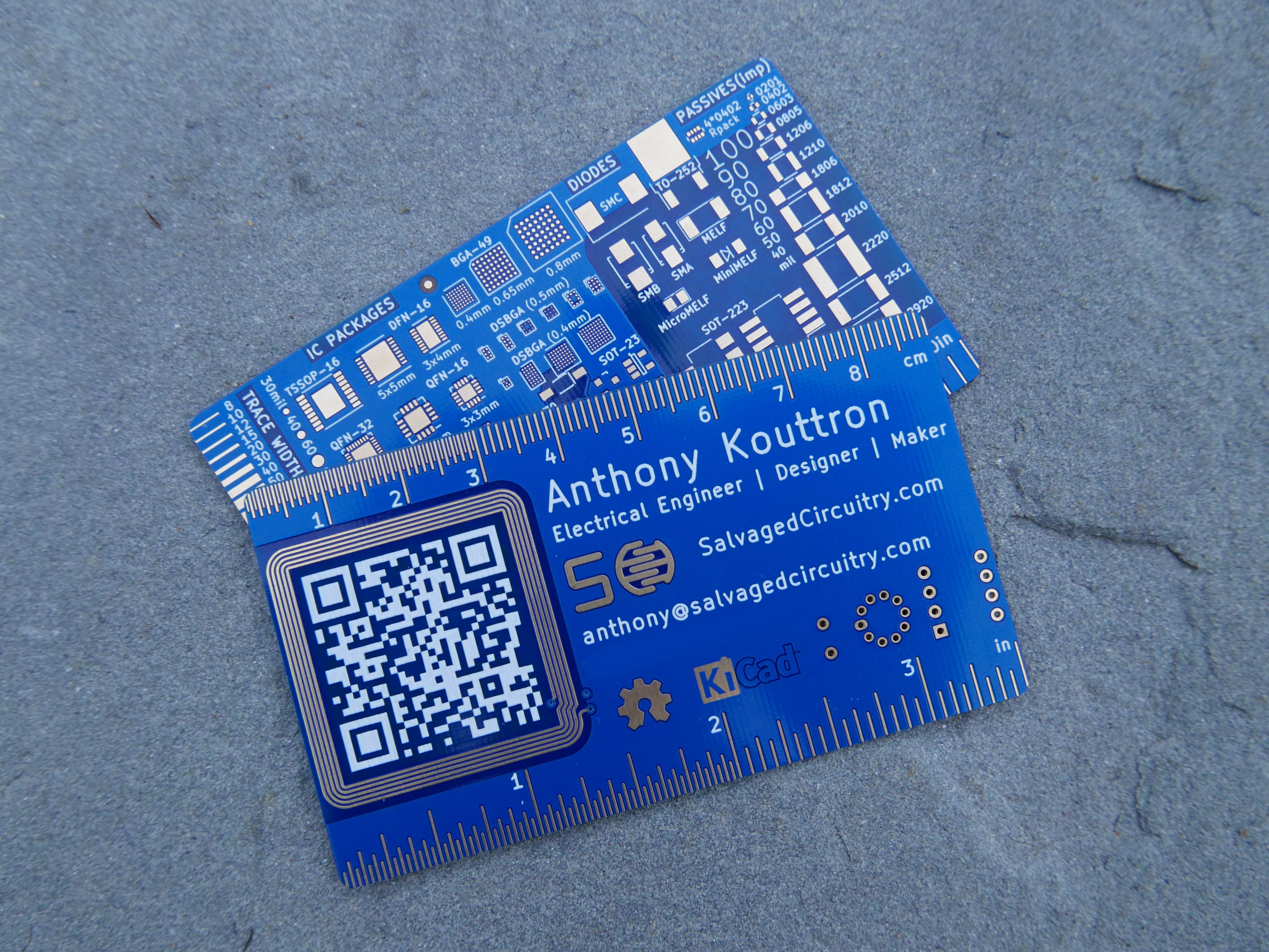
The concept of scale is also extremely important. Sure, that trace width gauge looks great from being zoomed in at 1000x, but when rendered to actual size, it's far too small and no one can read it! These are the main issues when making a tiny reference card. I found that the included 3D viewer in KiCAD is pretty fantastic for getting a decently accurate representation of the board. The 3D viewer enables you to scale the pcb small enough to exactly match the size of a business card by enabling orthogonal projection. This is the render on my 30in 2560x1600 lcd and the actual business card side by side. Nearly spot on. Using the 3d renderer, an optic and a caliper (for referencing font size on other rulers), I was able to create a pretty legible PCB business card without needing to send away for boards multiple times. A true life-saver.
I really like the use of soldermask pullback to highlight titles on the Digi-Key 12in rulers which gives that nice contrast-y two-tone color scheme, so I adopted it on my design. Also, a big shout out to Digi-Key for creating a dedicated Digi-Key kicad library with footprints, part numbers and links to part datasheets and Digi-Key part pages. This is extremely helpful.
Traditionally, footprints are designed to aid in the bonding of components to the traces on a circuit board. You line up the component to the footprint on the board, add solder and bam you're good to go. A footprint file consists of copper landing pads, specified soldermask pull back around the pads and a courtyard to prevent a copper pour in a specific area. The copper pads are connected to a series of copper layer nets which connects different leads of a component to different parts of a circuit. The soldermask is the negative of the copper footprints and serves as a basic insulator while preventing unwanted solder bridging. If you are making something non-critical like a ruler or business card it's not that important if a the footprints are floating and are not part of a copper layer net, as the PCB will never be used as an actual circuit.
The same way footprint files can be used for standard components, footprint files can be used to create PCB artwork. With the combination of copper pull back zones, soldermask pull back zones and traditional silkscreen, a layout designer can really get creative, such as this astro themed front solder mask. If you want to get crafty with PCB making, combining the soldermask pullback technique with fancy copper pad coatings such as ENIG (electro nickel immersion gold), will really make your designs pop and push your pcb from just-any-old-pcb to artwork.
Using soldermask pull back techniques, a myrad of common component footprints, custom rulers and useful size gauges, I created my first successful revision of a PCB business card. Even though my fingers were quite numb from constantly using [ctrl]+[m], I somehow managed to fit in four variations of each chip package on a single side. I spent a while moving components about trying to find a good middle ground for the density of components. This revision offered the best balance of usability and legibility.
KiCad Specifics
When I first started this project I was using KiCAD 4.0.6. This version, while very functional, caused me great frustration in use because the user interface was such a far shot from any other program I had used. While I have used programs with even worse interfaces that only allow for one saved undo (ahemm, 1990s Cadence Virtuoso) this program seemed unreasonably annoying to use. In PCBnew, the layout aspect of KiCAD, the cursor had this weird memory feature where if you right clicked a part to find out additional options and then clicked away from the right click drop down, it would bring your cursor back to the original location where you right clicked and close the drop down. The same thing would happen if you left-clicked a footprint and a drop-down appeared, but in this case your cursor would bounce back, the drop-down would not close and you had to hit ESC. The interface designers obviously wanted you to get used to opening something and immediately hitting the ESC key to properly close. Then you could proceed. This is so very different from any normal window navigation it's unbelievable that this methodology was ever implemented.
Kicad 5.0 PCBnew removed this cursor issue and implemented a lot of great new features. You can now measure anywhere on the canvas, move parts exactly (by coordinate or value), position parts relative to a point and use a graphic polygon tool to draw filled graphics on any non-copper layer. The layers manager now allows for toggling of through-hole pads, tracks and the worksheet outline too. Other welcoming new features include the ability to flip boards, export as a .step for mechanical assembly, and additional render options for the toggling of 3D through-hole or 3d SMD parts. The footprint editor also improved and added the ability to import .dxf files. I actually used every single one of these new features as well as the invaluable new hotkeys for the 3d viewer. If you are even questioning it, now is the right time to switch to Kicad 5.0.
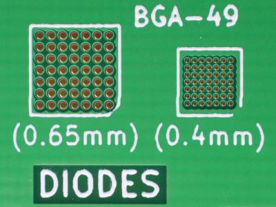
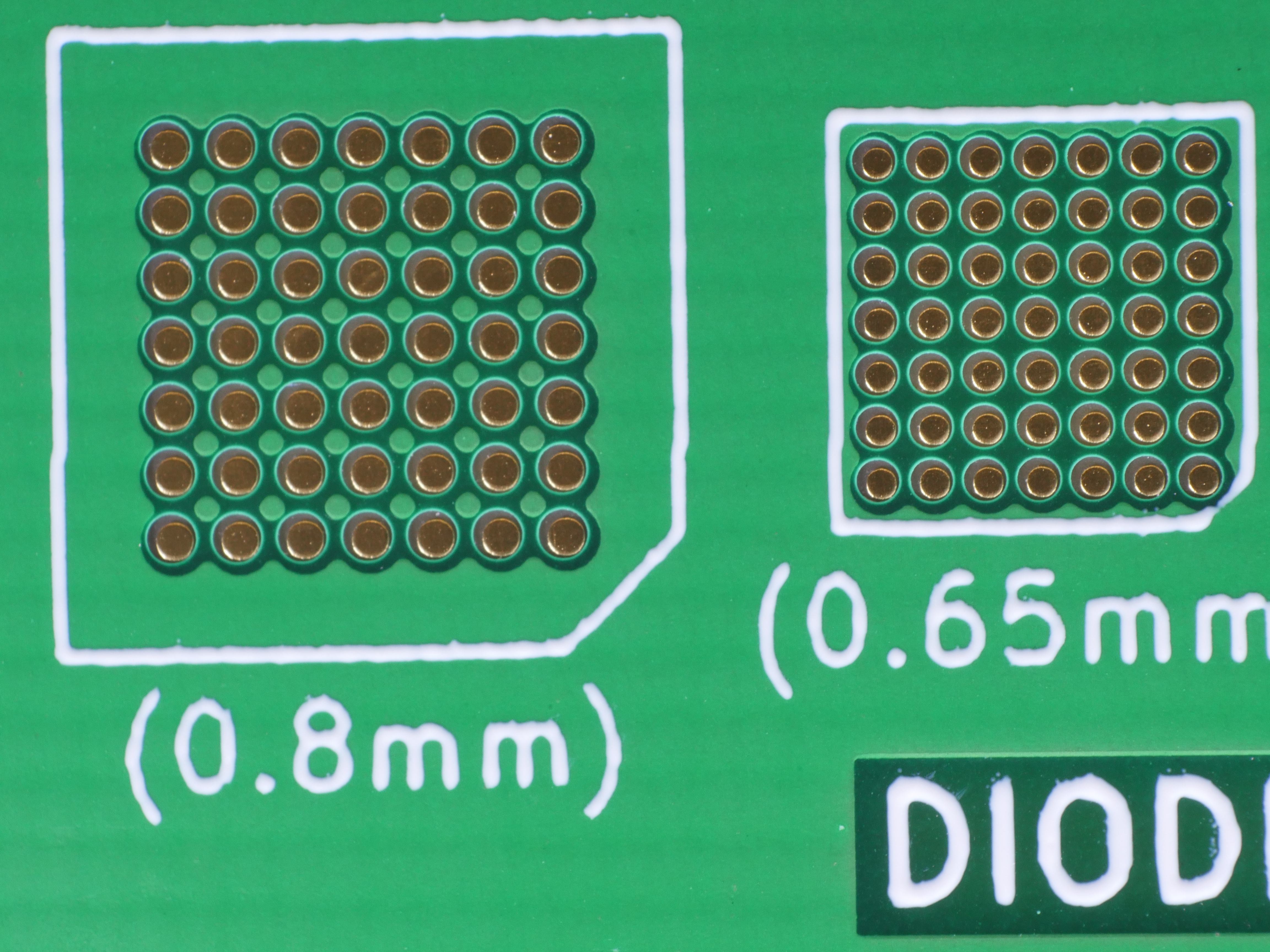
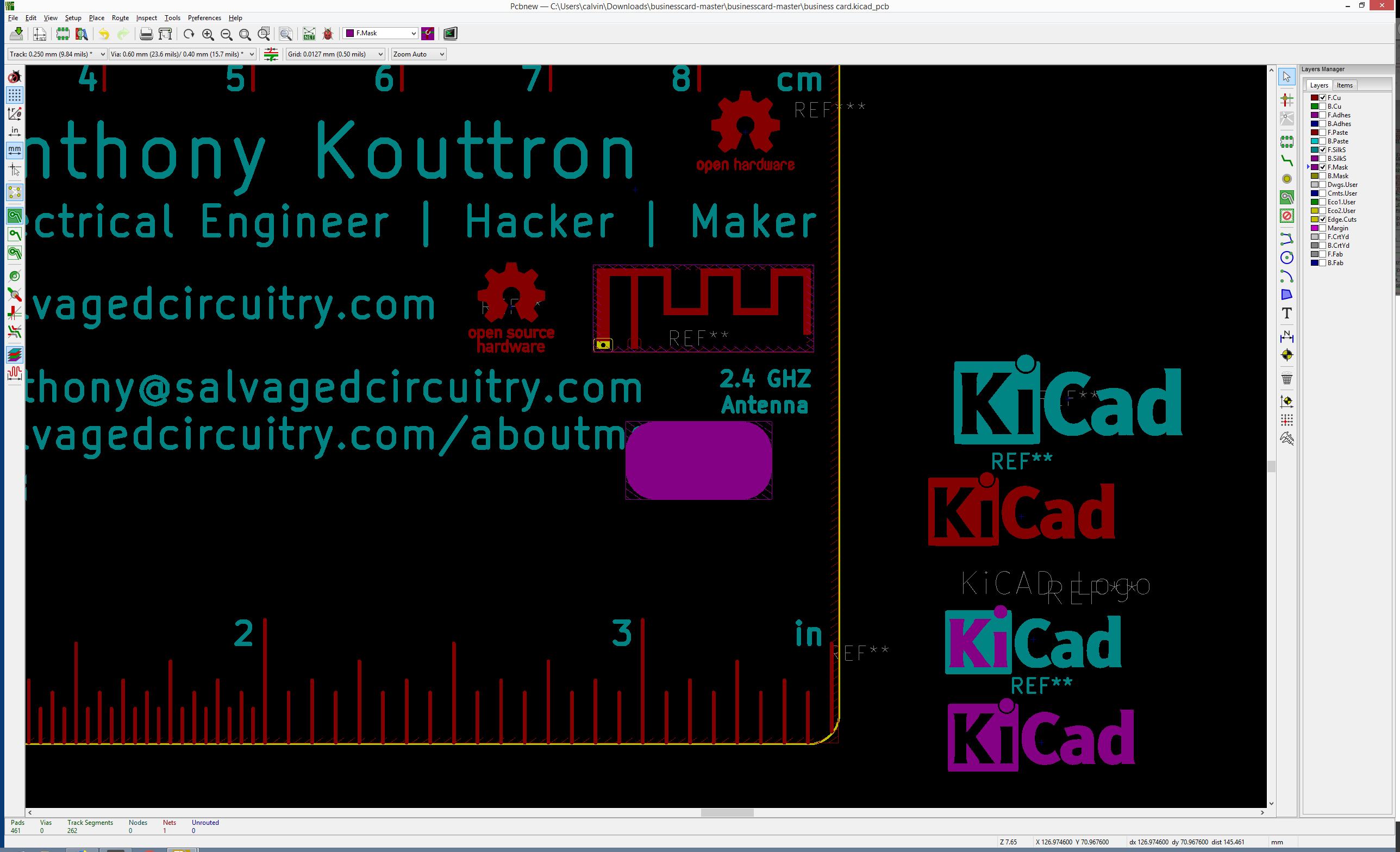
The original file made by Brian was composed in Kicad ~2 so the footprints look different than the most current Kicad Library. One really great little surprise with Kicad 5.0 was the additional 49 pin 0.4mm pitch BGA package footprint. Now my 49 pin ICs range from 0.8mm, 0.65mm and 0.4mm pin pitches!
To get started with this project and Kicad, it is best to get familiar with the five programs that makeup kicad: EEschema (schematic layout editor), symbol editor, PCBnew (layout editor), footprint editor and gerber viewer. PCBnew is where you will spend most of your time. The biggest time saver with using any software is watching demo videos and of course learning the shortcuts. Here's a list of the most invaluable KiCad shortcuts needed for this project:
Within PCBnew:
- B = fill
- Ctrl B = remove fill
- Ctrl M = move exactly
- Alt + 3 = show 3d render
- Tilda = highlight net --> makes everything darker. Hit again to remove
- Ctrl + Shift + M = measure
- View > Flip board view (no hotkey yet)
- Help > List hotkeys
- PgUp = Switch to top component layer (F.Cu)
- PgDn = Switch to back copper layer (B.Cu)
Within 3D Viewer:
- Z = Show board on side one
- Shift Z = Flip board
- Tab = Rotate
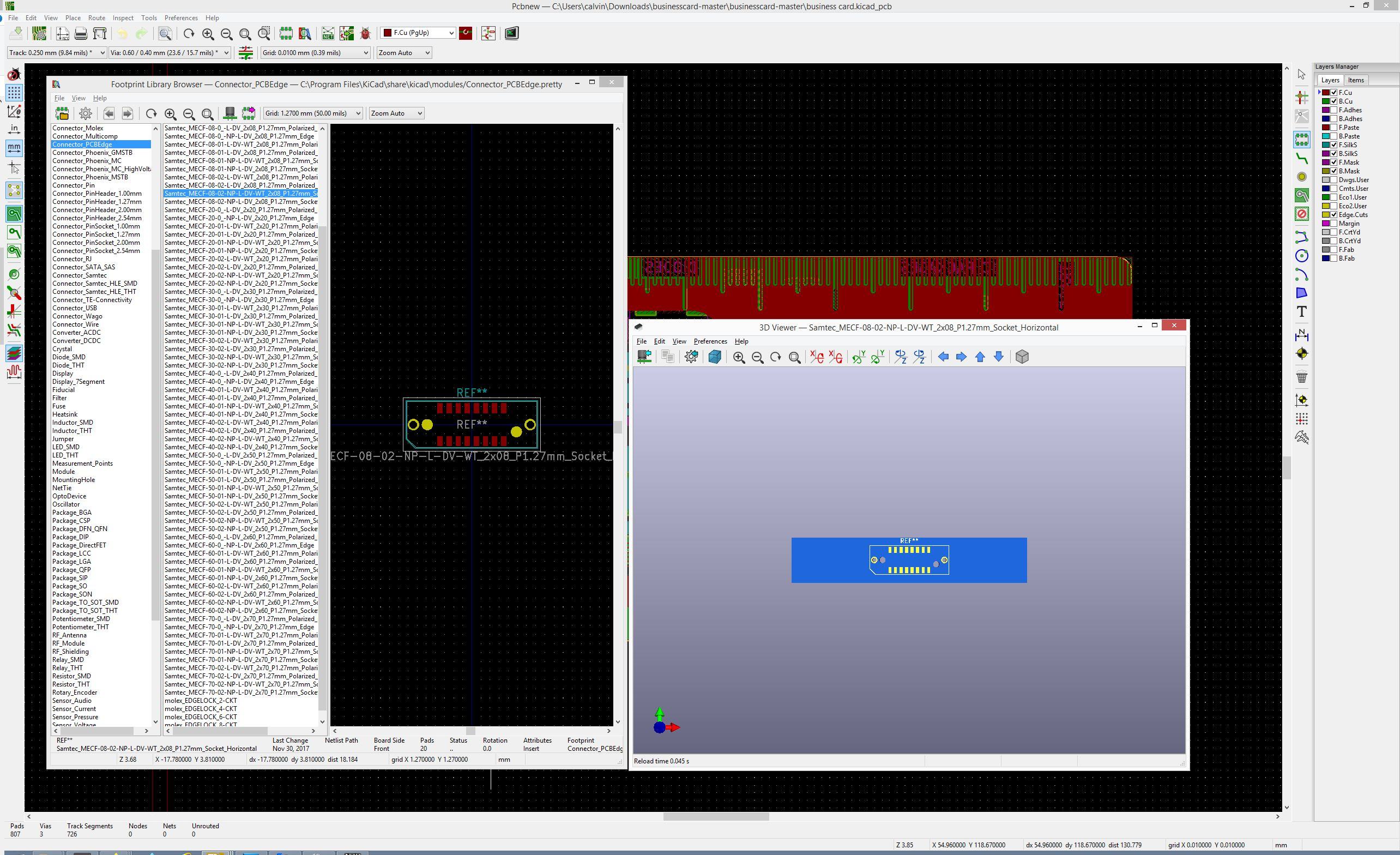
A good portion of this project involves the tedious use of the measure, move tool, and switching layer tool, but your biggest friend is the included PCBnew footprint libraries. There are hundreds of SMT and through hole footprints available, from connectors to terminal blocks to even old school can oscillators. You can even view the footprint and 3d model of the footprint side by side before placement! How convenient is that!
Generate Gerbers and Drill Files
Once you are satisfied with your Kicad project, go ahead and begin the export process. Go to File > Plot. Select gerbers in the top right under "plot format." Set the gerber output directory to a new folder. Select yes to "do you want to use a path relative to..." so the path works for other people who may want to download / modify your project if you chose to share your project.
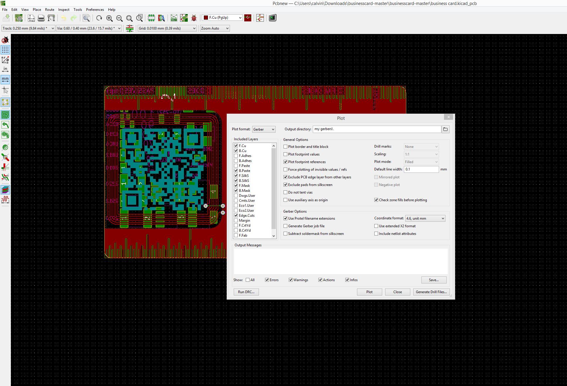
Settings:
- uncheck "plot footprint values"
- check "plot footprint references"
- check "exclude pcb edge layer from other layers"
- check "exclude pads from silkscreen"
- uncheck "subtract soldermask from silkscreen"
- check "use protel filename extensions"
- Included Layers:
- f.cu
- b.cu
- f.silks
- b.silks
- f.mask
- b.mask
- edge.cuts
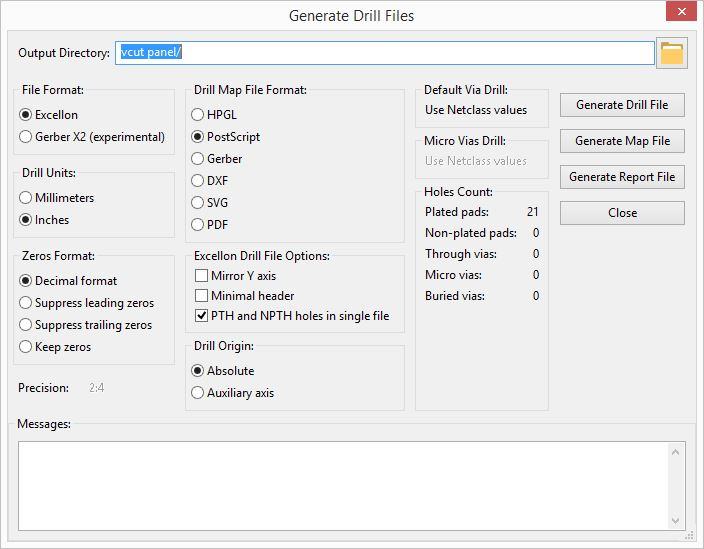
Generate Drill Files
Drill files are used as coordinates for drilling and jig borer machines to make incisions into your PCB. Select "Generate Drill Files..." on the plot window. This will bring up another menu.
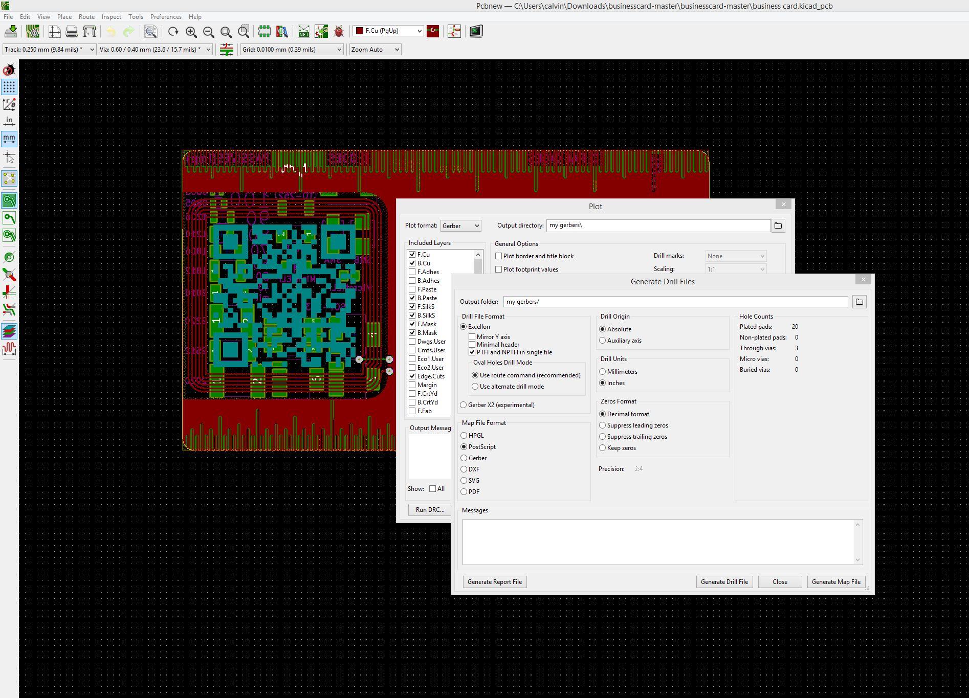
Settings:
- check PTH and NPTH in single file
- Drill map file format: PostScript
- Drill units: inches
- zeros format: decimal format
Now click Generate Drill File and you're all ready to zip up your gerbers and drill files and send them out to your PCB vendor of choice. For reference, here are two other great guides on Kicad output file generation from Oshpark and Digikey.
Inspection, Inspection, Inspection:
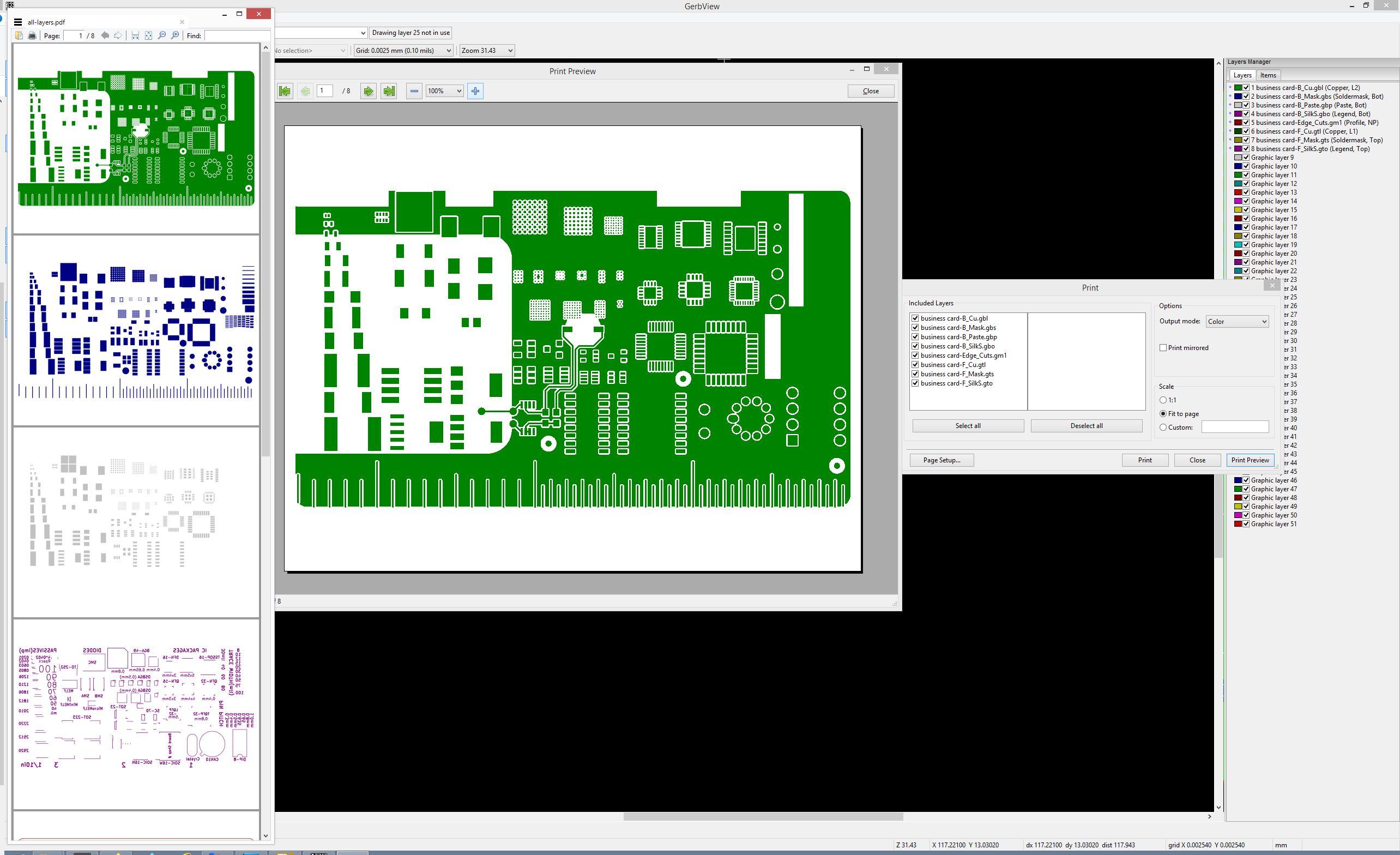
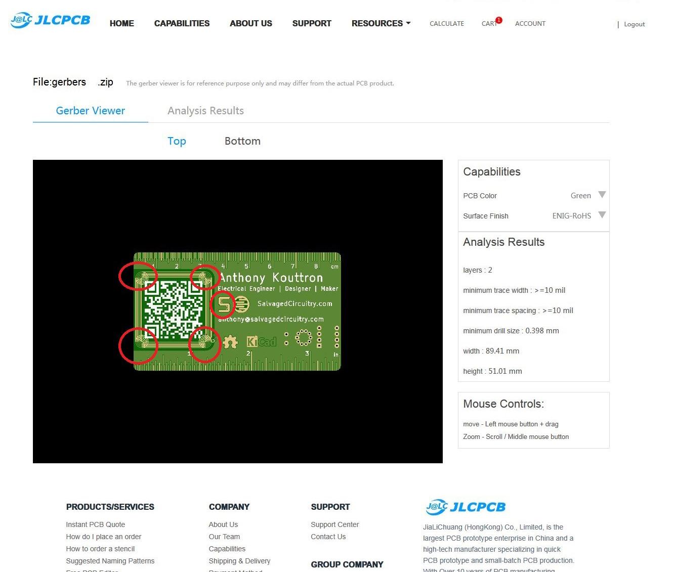
It's sound practice to double check everything before shipping out for production. A good place to start is from the outputs: the gerbers and drill files. Unzip the gerbers and drill file and open them with different gerber viewers. I used both the built-in KiCad "Gerber Viewer" along with the excellent GerbV gerber program. Simply load the gerbers into the programs and inspect. I like to load the drill file and edge cuts first, then add all the rest but order doesn't really matter.
Start by inspecting each layer one-by-one. Disable all the imported layers and enable the edge cuts, drill file and front soldermask. look to see how the drill holes and soldermask keepout line up. Do they look centered? if not, something is clearly wrong in your pcbnew project file and you'll need to go back and correct it. if all looks good, disable the front mask and toggle on the back mask. Do the drill holes line up? Toggle off the mask and toggle between the f.cu and b.cu layers, checking to see if drill holes and pads line up. The idea is to take advantage of contrast to point out any errors that you might have missed when creating the board as a stack inside pcbnew.
Another nifty trick is to compare all layers using file > print and print preview. Select the color option. This will create a multi-page preview of each layer printed one after another. This provides a nice contrast of layer vs white background to help you spot any errors or mistakes that you may have overlooked.
When I'm confident my gerbers resemble what I want, I like to "sit on it" and wait for a good solid 20-30min before sending them out. This way I have adequate time to mull over and accept the completed nature of my design in my head. I literally save everything, close down all my pcb software and do something completely different. Sometimes this belief that you are done clears up head space and reminds you of another idea you had for a minor revision or allows you to think of a completely new design. This is how my backlit salvagedcircuitry logo came to fruition. I was originally perfectly content with back illuminating the open source hardware gear logo. I sat on it for a bit, came back and added it to the second revision.
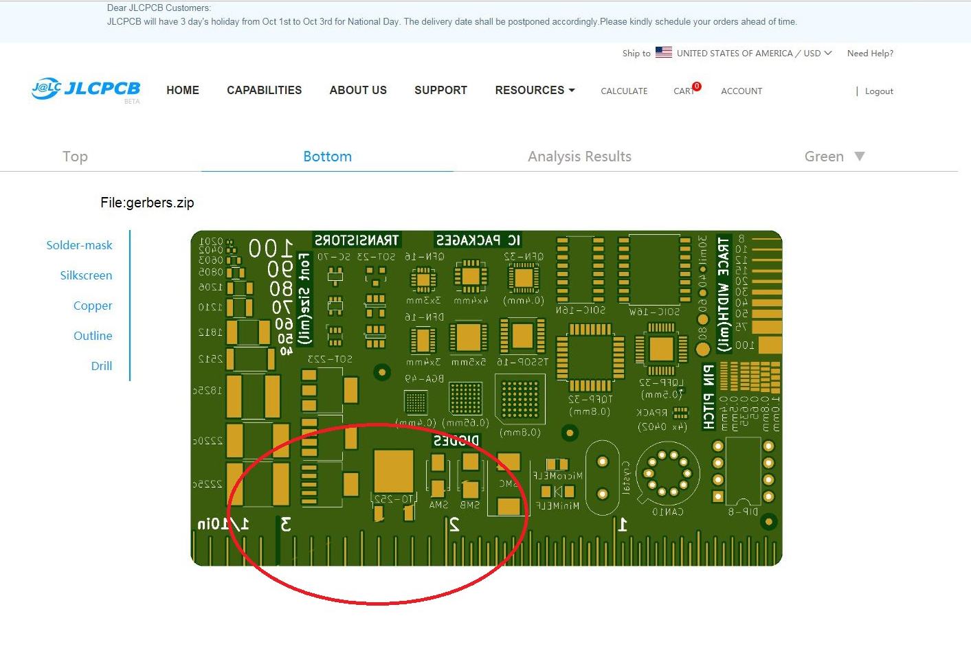
If you're submitting a ~40+ board order, it's a good idea to flag the PCB manufacturer to send an image of what the board looks like on their end. It seems that a lot of board houses use their own proprietary gerber tool or some mashup of a currently available gerber tool.
I had an issue with the included JLC online gerber viewer. It showed some circular traces intersecting themselves in random places throughout the board. That did not show up in either of my gerber programs. It would have been catastrophic if I received 150 boards with semicircular ruler traces. Try explaining curved ruler traces to someone!
SHIP IT! PCB Ordering Process:
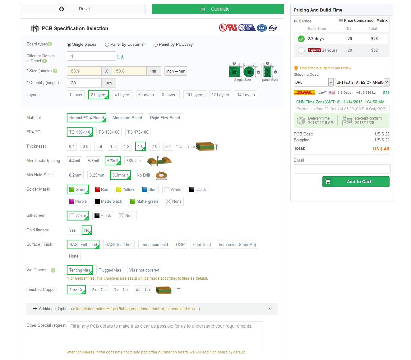
With the gerber and drill files all zipped up, and the gerber files checked for consistency, you are now ready to ship out your boards to final production! Now comes the decision on board production costs. How much are you willing to pay? Where do you want your boards made? There are a myriad of PCB vendors available. A majority of the low cost vendors are located around shenzhen and various chinese providences, but there are also several great vendors in the USA and Germany that can output very high quality boards. Since these business cards are by no means complex or in need to critical tolerances, I chose to manufacture the boards at two inexpensive PCB vendors in China.
This image represents the user interface used by a majority of the inexpensive chinese board manufacturers. Almost all of these board houses suspiciously use the same near-identical interface for calculating cost per feature, which is rather strange.
Here's a breakdown of what all these features mean for someone just jumping into PCB design:
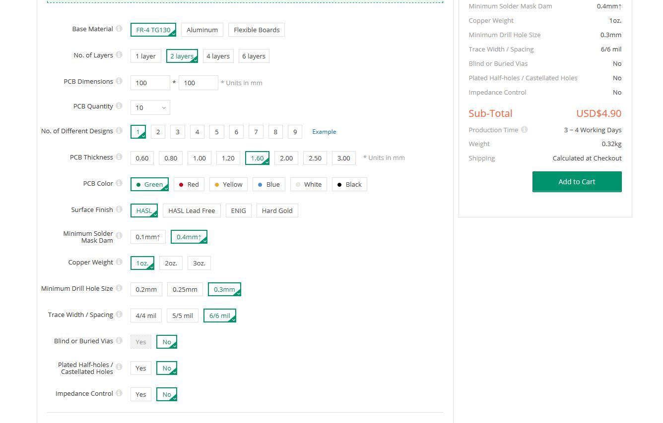
- MATERIAL: You want to choose Normal FR-4. FR4 is a Fiberglass based insulator pcb and is the most commonly used PCb material. Aluminum board is aluminum backed PCB which is useful for custom high-power led boards that will dissipate a lot of heat and need good thermal conductivity. Rogers board is an overarching term used for boards with a different insulating material than fiberglass. Usually a teflon based or other high tolerance material that is very useful for Radio Frequency applications. Rigid flex board is for flexible Pcbs commonly found in high density digital designs.
- FR4-TG: This is the thermal properties of the PCB selection. TG 130-140 is fine, you will not need to reflow this board as it is unpopulated.
- THICKNESS: Normal PCBs are usually 1.6mm thick. For business cards, you want something thin. The best business cards are usually 20+ point thickness, which is 20 thousandths of an inch thick. This is about 0.5mm thick. Most board houses have a sub 1mm thickness available. 0.6mm-0.8mm is a good trade off, and a lot of board houses won't charge extra for 0.8 or 0.6mm. 0.4mm is more expensive so avoid that.
- MIN TRACK SPACING: This is the minimum distance between traces on a board. Stick to 6mil track spacing at the minimum. Business cards need to be as inexpensive as possible, and this is not where you want to spend extra.
- MIN HOLE SIZE: stick with 0.3mm as smaller holes add cost.
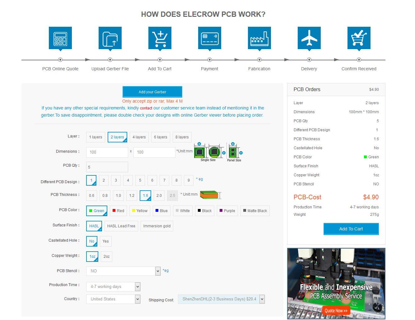
- SOLDERMASK: This is the coating that fills in the space between copper traces and prevents shorting. This is the "color" of your board. Choose anything that is not matte. Matte colors are usually more expensive and I don't believe they turn out that amazing. Most pcbs produced have a glossy finish and having a matte one may look odd and not be as durable to repeated handling. Most importantly PAY ATTENTION TO YOUR BUILD TIME ESTIMATE! Some soldermask colors are only run on a few days of the week, so your build time will go up by a day or 2 while the boards are on hold.
- SILKSCREEN: This is the color of the text on the board.
- GOLD FINGERS: This is a process where the exposed pins on a board are hard plated with gold. This is expensive and only needed for RF designs and boards that will be repeatedly removed/inserted like board-edge PCIe computer cards.
- SURFACE FINISH: This is the type of finish that will be applied on top of the exposed copper pads. HASL is the traditional cheap Hot Air Solder Leveling plating that applies on top of a pad. Leaded is cheapest, lead free is a bit more, Gold is even more and the other options are astronomical. OSP sounds like one to avoid. Immersion gold, or Electro-less nickel immersion gold is what you want for business cards. This is where you need to break the piggy bank. Gold plating will make any PCB project look fabulous. Gold plating is used on a lot of fancier pcbs not because of how it looks or pad quality, but because how flat gold lays on a pad. It allows for superior part leveling and solder wicking/adhesion.
- VIA PROCESS: Tenting vias is perfectly fine.
- FINISHING COPPER: 1oz is plenty for a board that will never be used. When doing PCb runs for actual boards, check the copper allotment from your vendors. Sometimes cheap board houses do not actually give you a 2oz copper board when you pay for it and give you something slightly more than 1oz, which is frustrating.
My Results
I originally tried out the "single pieces" production option to get an idea for how my boards would look by the default method. They came out far better than I expected. I thought I would be getting smudged, uneven silkscreen, terribly mis-aligned soldermask, and have a crap finish. To my surprise, the boards came out quite good.
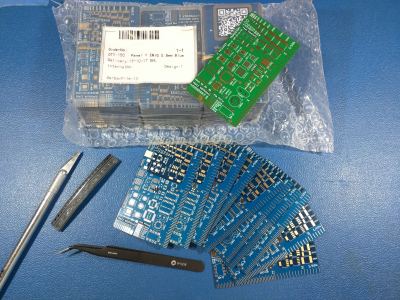
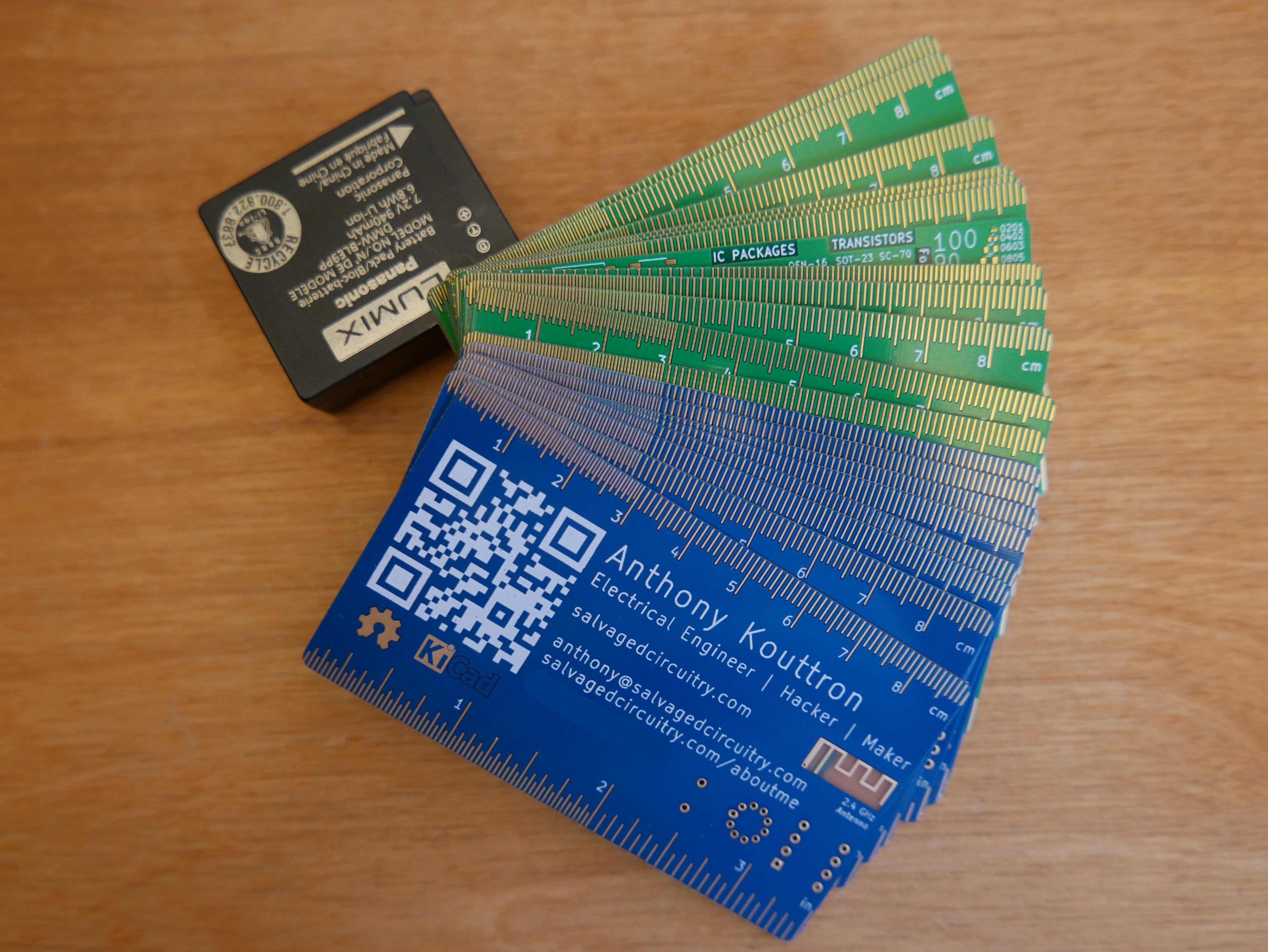
I spent $118 on 30 express production, express shipped business cards. I used Pcbway as the vendor for the blue business cards and they still managed to ship me my business cards in time (ahead of schedule) even though they were enduring an unexpected monsoon. That is frankly unbelievable. I still don't know how they did it.
The cards were unbelievably good. Look at how well the ruler marks line up. They are near identical to the Adafruit rulers. This photo doesn't do the rulers justice, as the lens used has a bit of barrel distortion. A truly rectilinear and well-corrected macro lens is needed to show how well they match up. They are spot on. I was completely blown away by the results and seriously wondered why more folks don't make PCB business cards. PCBs almost never come out this well on the first run.
At ~$3.93/card, it's understandable why this is not very commonplace. Business cards are usually made in advance by a corporate marketing department so I can't imagine they would bug an engineer to make promotional business cards for the entire company.
Besides this, traditional paper business cards are about 4-30 cents per card depending on quantity and quality. If I was not in a rush to get the PCB business cards before the 2018 OSHWA conference, I would have paid close to $2/card through PCBway, or half my original order. Regardless, this is still quite an expenditure for business cards.
Further Inspection
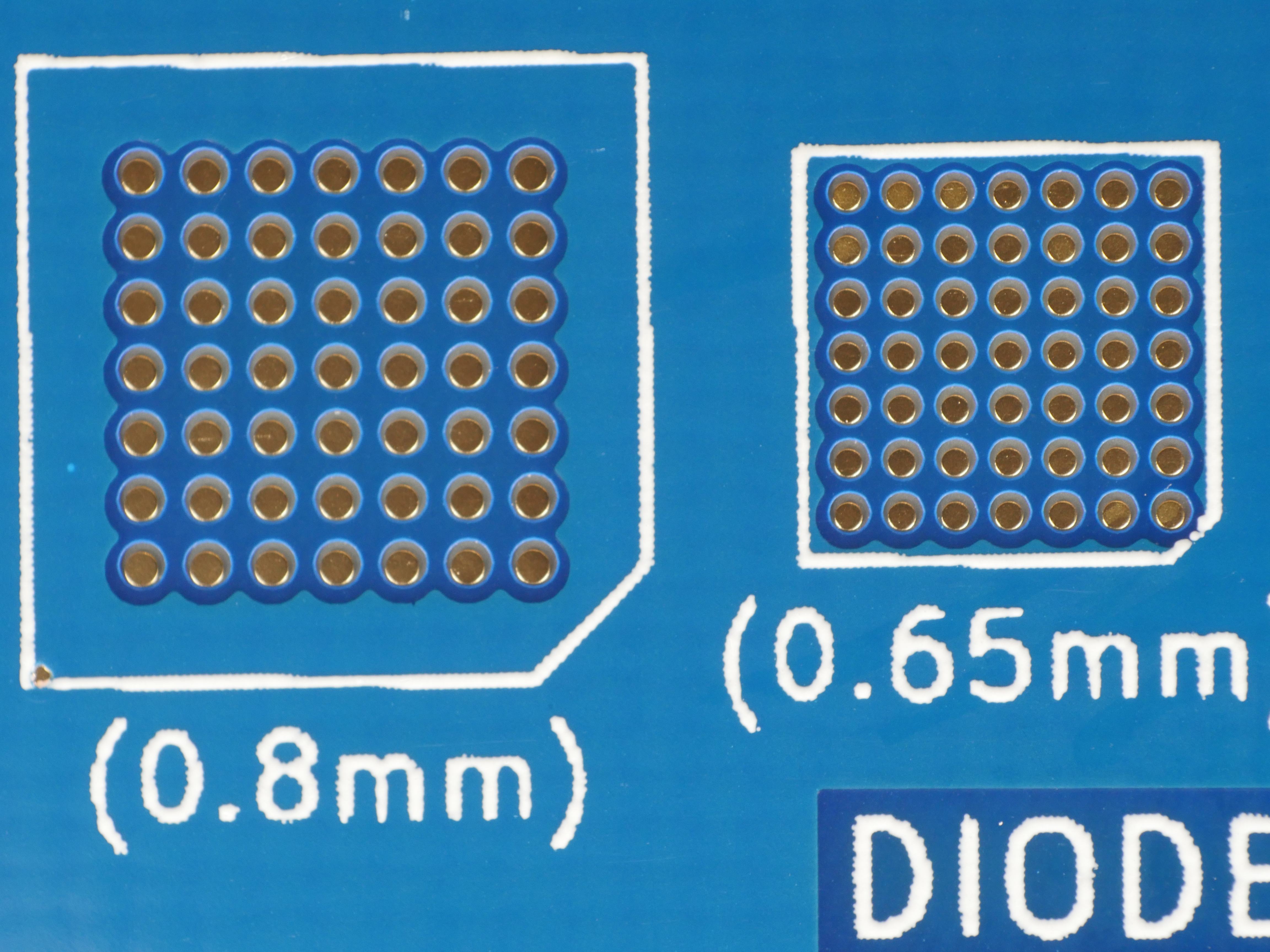
You can see there is definitely a bit of misalignment between the soldermask keep out and pads (look at those BGAs). It looks like one or two thou off. This may be a deal breaker for a high data throughput, large gate, multi-layered fpga based board, but it's totally overkill for a business card :D.
The silkscreen gets a bit thin in places though and the finish is not completely perfect, but it's good enough. The good news is that the silkscreen only gets thin in a few small areas of the board. Overall, the silkscreen has a very 1990s inkjet-like look.
Look at this excerpt. The trace widths look nice and crispy. The soldermask pull back regions look great and the test pads don't look too off. The results totally blew my mind in spots.
let's take a look at the green boards from JLCpcb. Starting off, the BGAs look identical in quality to PCbway. 1 or 2 thou off. Minute, but noticeable with magnification. Oddly, the soldermask is present between the pads of the bga 49, whereas soldermask was not present here on the pcbway board.
The silkscreen is very distinct with the JLC boards, but not in the best of way. It is very much applied in excess and makes some text hard to read and very bold. Whereas the pcbway silkscreen looks ink-jet like, this one looks quite over-done and in great excess. There is even a very tiny height difference when you feel the silk screen on the JLC cards.
Just like the pcbway one, the trace widths look very sharp and the test pads dont look that far off center.
The mark quality on the rulers look pretty even and uniform, so a major plus there.
Something very pronounced on the JLC boards, was the amount of silkscreen splatter. There were tiny white dots left all around the board as leftovers from the silkscreen process. It's not super noticeable, but under close inspection it's definitely there.
After several rounds of comparisons, it is clear that both vendors are very close. However, I did notice something that separated the two. It seems that the resolution of the blue PCBway soldermask is not as high as the green soldermask resolution of JLCpcb. There is no blue soldermask around the pads of either QFN-32 package on the pcbway board, but there is green soldermask around the pads of the QFN-32 package on the JLCpcb board. To me, this is not a big deal as these will never be soldered, but this may be a deal breaker for some designers who want to make sure their solder paste doesn't bridge between pads. In reality, this is not a fair comparison, as green is a lot more common of a soldermask than blue, and the machine that pcbway uses for the blue soldermask may be a lower run, lower resolution machine. PCbway green soldermask may be better. After contacting pcbway, it looks like it's more of a policy than a resolution limitation. Pcbway doesn't bridge soldermask if an opening is less than 0.25mm or 0.2mm.
By all means, these boards are not perfect, but I'm not paying Advanced Circuits or Wurth Electronics prices for business card sized PCBs. Wurth wanted $252 before tax and shipping for 20 business cards. I'm sure the quality of the wurth pcbs are godly, but there is simply no way I would pay that for business cards. Crazy! The second batch of PCBs (green ones) via JLCpcb was $67.78 for 50. This is about $1.36/card which is a lot more reasonable. I am completely stoked with how both vendors performed and now I am completely sold that this was a good idea and worth the time and effort. NOTE: I am not paid by any PCB vendor and have not received any promotion for this PCB writeup from any vendor. I would surely love to test out these business cards with Wurth, Advanced circuits, OSHpark and other top tier vendors to get a good idea of the variance in PCB manufacturing.
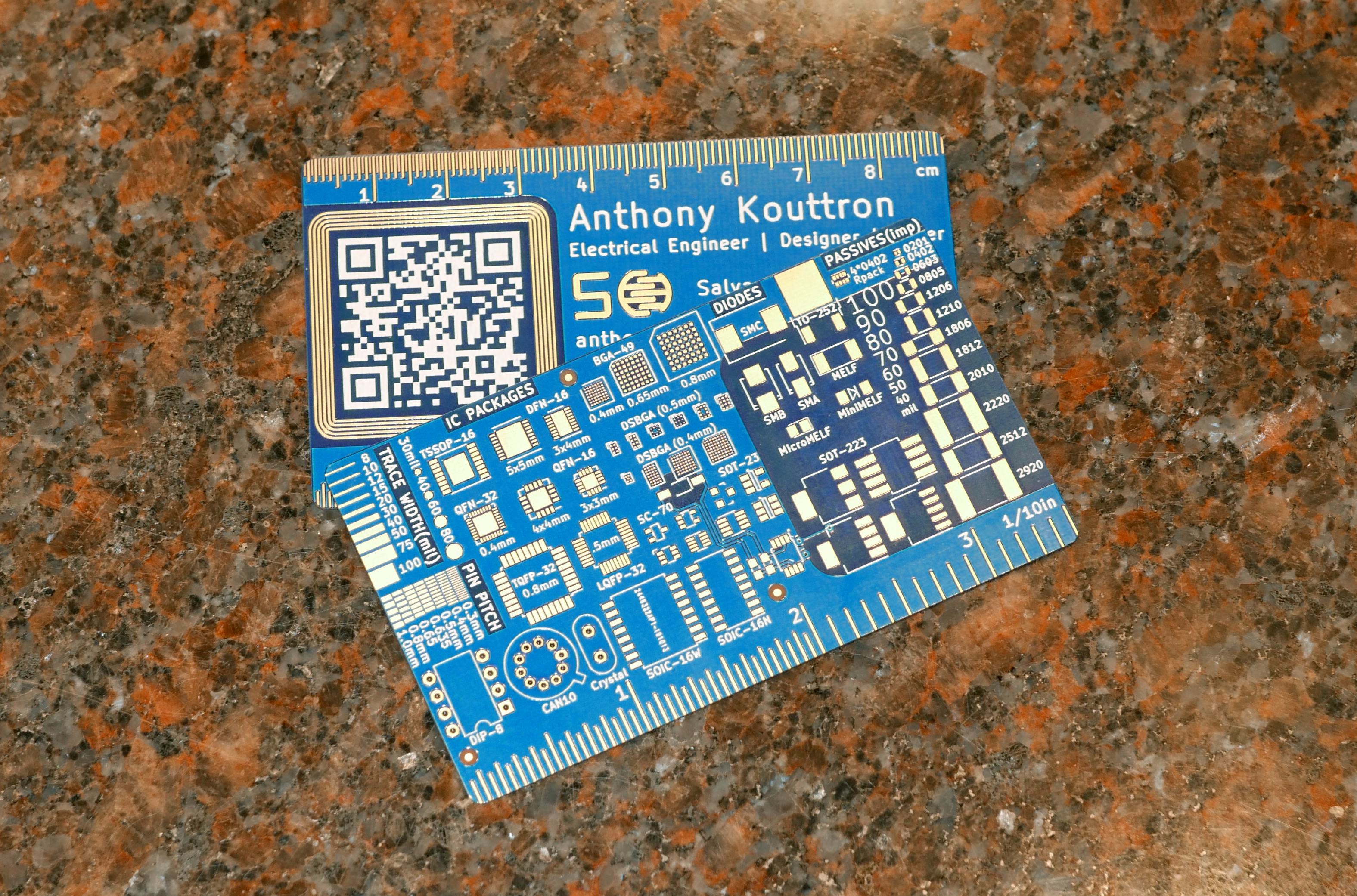
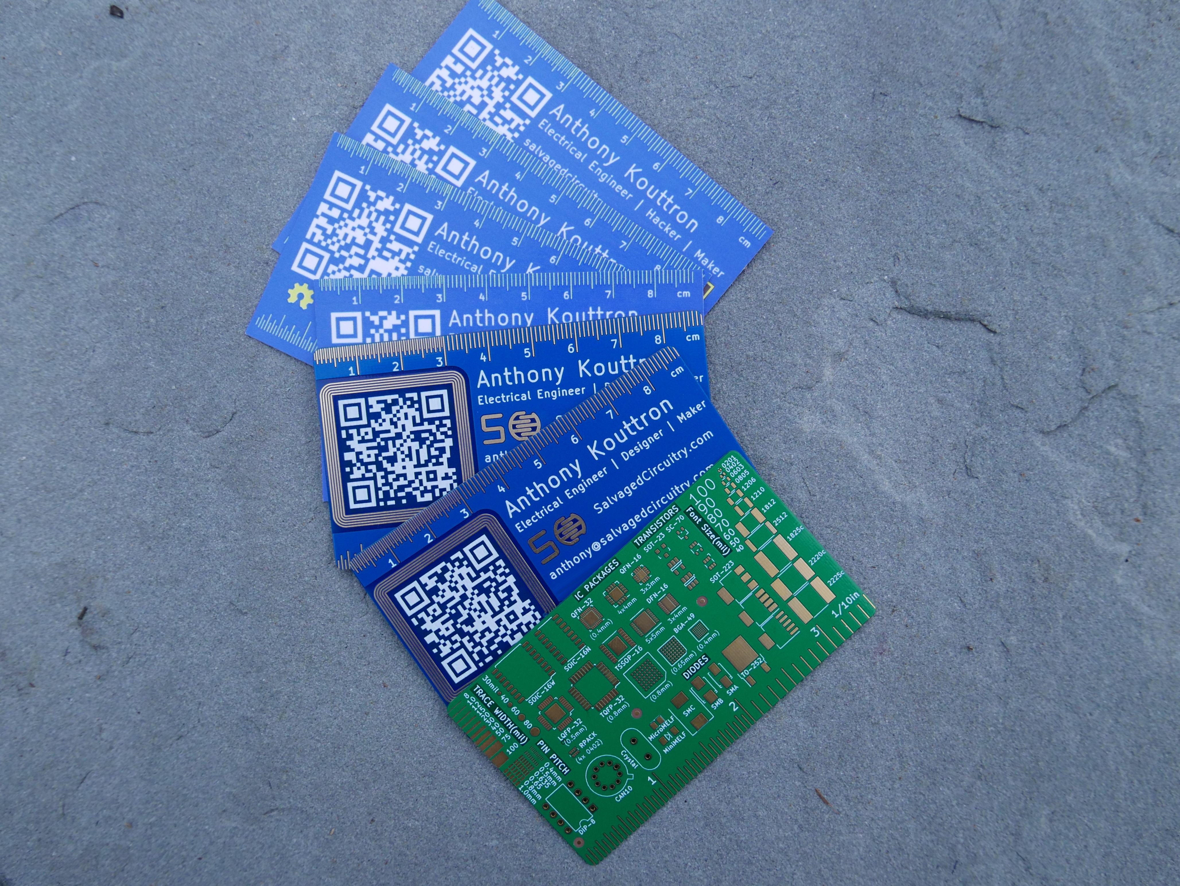
Revision II: NFC edition
My PCB layout business cards served me well and were a good conversation starter at conferences and events. As I came across more and more business card designs, especially those integrated NFC based business cards, I knew I was in for a redesign.
Loann Boudin's excellent PCB business card with NFC really pushed me toward Revision II as I was unaware of any single package NFC chips that could handle phone to coil handshakes, without the need of jtag reprogramming. I was blown away by how simple and quick it was to implement the tiny NFC chip in my design, program it with an andorid NFC app, and have the card up and running. I thought the off-the-shelf NFC tags were the only economical option. Special thanks to Eric Kuzmenko for sending me the instructables link and Loann for the excellent writeup.
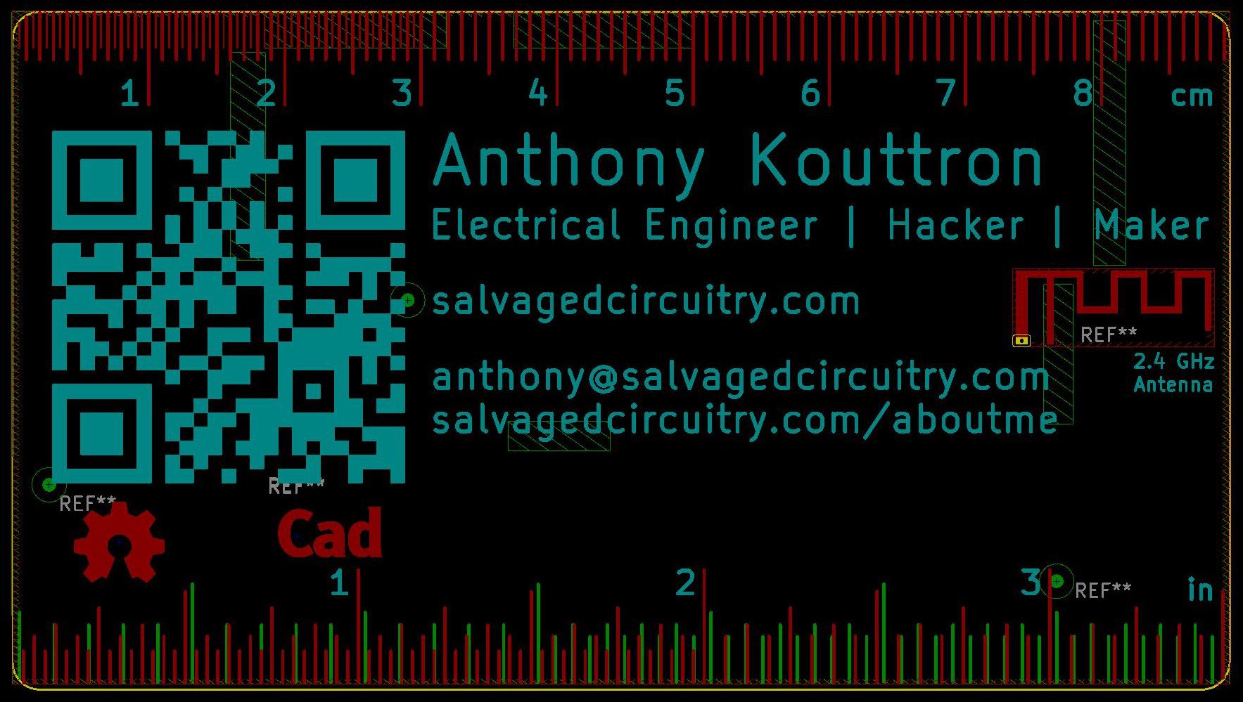
This is my latest and greatest business card. It implements QR, NFC, the same three rulers, but a whole lot more packages - all while maintaining a legible silkscreen. I also added in even smaller packages, such as the 0.4mm pitch dsbga footprints as well as more footprint variations. It's powered by a tiny NXP NFC chip with power harvesting capabilities. The small tssop-8 package is still big enough to hand solder, which is a major plus. This chip handles all the NFC handshakes and can harvest enough power from a phone to power the chip, transmit a web address and blink an LED. The NXP chip even comes in a XQFN-8 package measuring 1.6x1.6x0.5mm high. Crazy! If I ever decided to switch over to a stencil and paste assembly process, that's my primary choice.
The NFC coil design implemented was based off the suggested ISO/IEC 14443-1 criteria for NFC coils. The major benefit of using a specific "class" coil is that the example coils are thoroughly tested and characterized, so you know they will work flawlessly within an NFC design. Here are some very inclusive antenna design guidelines found in application notes from three major semiconductor manufacturers. These have more information about the 6 coil classes (class 1-6) and the appropriate antenna sizing calculations.
Of the 6 defined coil classes, I selected a "class 4 coil" measuring 27x50mm, as it actually fit within my board space of 89x51mm. Unfortunately, the class 4 coil was a bit too rectangular for my layout design, so I modified it to be more square to fit in better with my business card. I compensated by adding another turn to the coil as well. Conveniently, the NXP Guide to designing antennas for the NTAG I2C plus includes the design files for class 4 and class 6 coils, so I didn't have to manually create a footprint in kicad. The coil design files turned out to be eagle .brd files, but the awesome Kicad developers included a kicad-to-eagle converter in Kicad 5.0+, so crisis averted. Thanks KiCad devs!
One unforseen problem I had with the coil is the curved corners. At this point in time, Kicad 5.0+ can not make or edit curved copper traces fluidly. To draw a curved line, you need to integrate dozens of points along a line into a curve-like shape, very similar in principle to how a gerber file read-out would look: a series of X,Y coordinates. Because I did not want to painfully redraw these curves manually, I added a square coil on the inside layer to avoid making a curved corner. I plan to update this design when curved trace capability is added to Kicad. If one is very invested in kicad of skilled in python, I believe it is possible to implement a curve drawing function using the python plugin module for kicad. I opted not to do this because it is a very minute issue that would have minimal impact on the coil, considering how many pads on the flip side are causing interference.
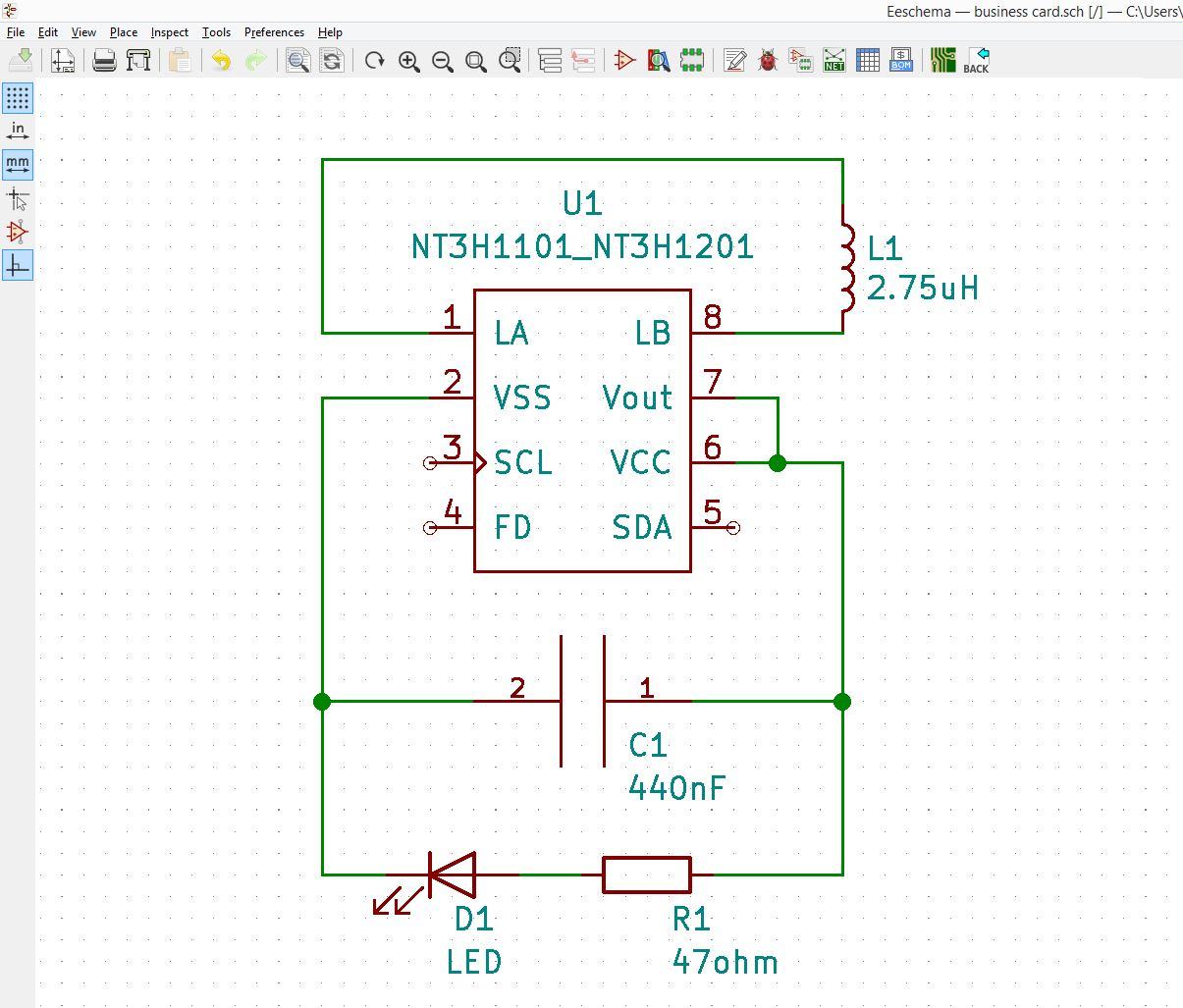
Here is the circuit diagram of my business card. It is incredibly simple and is based off the guidelines specified by NXP. I went with 0603 components so I can still easily hand solder them in place. A 220nF capacitor was chosen as NXP recommends a minimum of 200nf across VCC and GND. This value was doubled to 440nF to allow for the use of a higher current consumption LED. A green led was chosen because the forward voltage across a green led is ~2.1v. A 47ohm resistor in series with the LED was used. The resistance value was calculated based on R = (Vcc-Vled)/ Iled where Vcc is the supply voltage (tied to the Vout energy harvesting of the chip), Vled is the operating voltage of the led, and Iled is the current through the LED.
You may have noticed a change in style with this card. That curved contrast-y bit is a copper pour keepout region, around the NFC coil. In order to preserve the permittivity of that portion of the card, the internal copper layers had to be pulled back to reduce interference between the coil and neighboring copper structures. This ensures a magnetic flux between the coil in the phone and the coil in the business card.
Of course, there are still a bunch of smaller copper pads on the back, partially mitigating this design practice. Because this business card will be handed out with or without components soldered in place, leaving almost 1/3 of a card side blank was not an option. I chose a happy middle ground where a small amount of components were placed over the back side of the coil. It's not ideal, but all this card has to do it transmit a website and make an led blink. An imperfect antenna should work just fine.
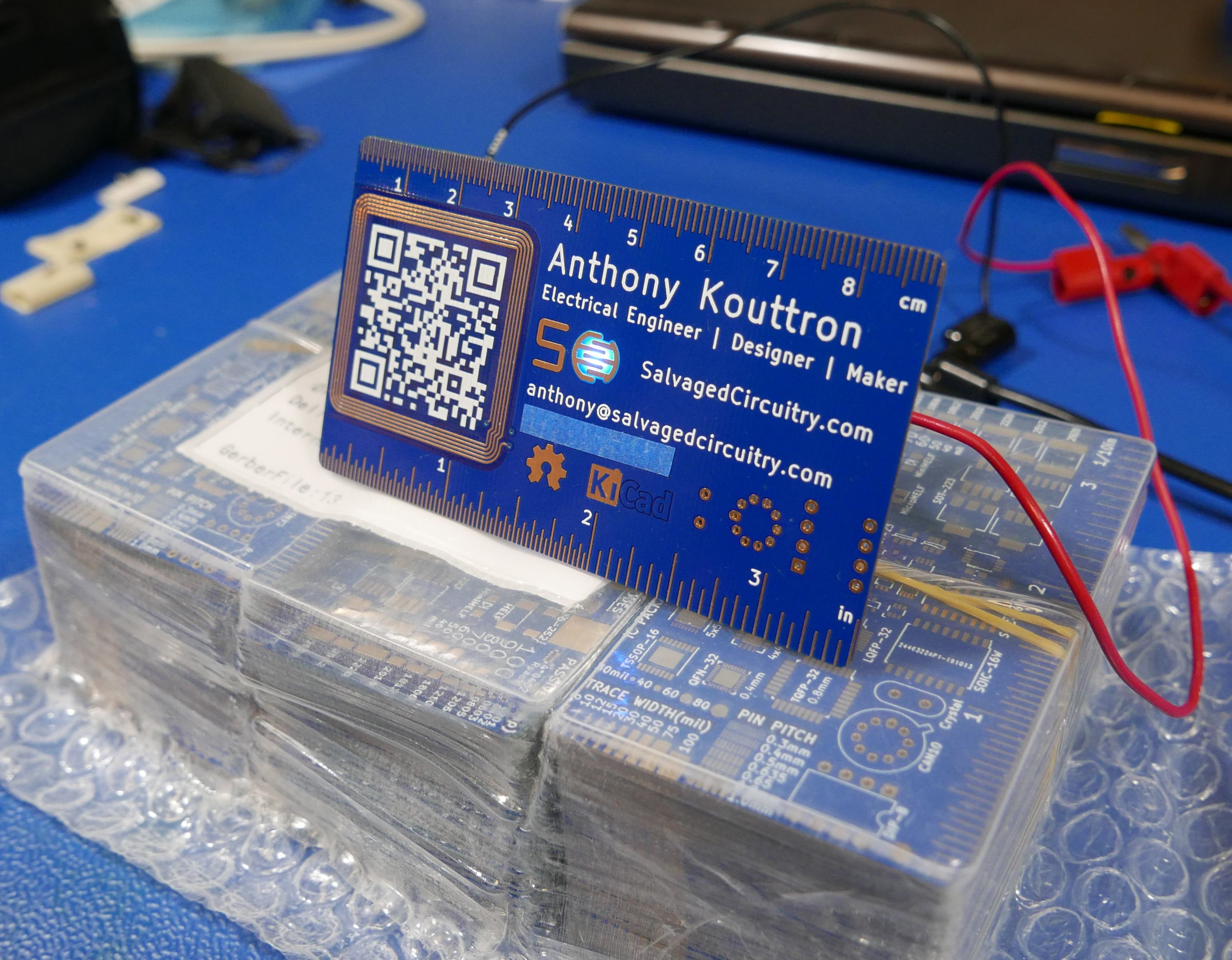
Lastly, I added in a backlit salvagedcircuitry logo to add that extra bit of flare to the card. I always liked the look of backlit illuminated PCBs, even going back to the days of simple double layered 80386 motherboards. There is just something about the way fiberglass prepreg layers evenly diffuse light and make the pcb act as a single color diffuser.
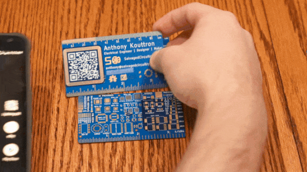
Here is the business card in action. Works like a charm.
Kicad Files & Gerbers
My latest business card was designed in KiCad 5.0. The design files are free to download. If you haven't checked out KiCad, now's the time! Check out the amazing work of the KiCad devs on their ever-growing changelog. If you are having trouble using KiCad, comment on the KiCad Forum or try watching some recent online tutorials.
Kicad Files
Duplicate Kicad Files on GitHub
Special thanks to Brian D. Carlton for creating an awesome KiCad business card template. This project is an extension of Brian's original project and is appropriately licensed under a Creative Commons Attribution-NonCommercial-ShareAlike 4.0 International License.
Please note, when having PCB business cards made, use ENIG or PBfree coatings. Do not hand out HASL lead solder based business cards to people. Lead is not safe if ingested. Don't be that guy.
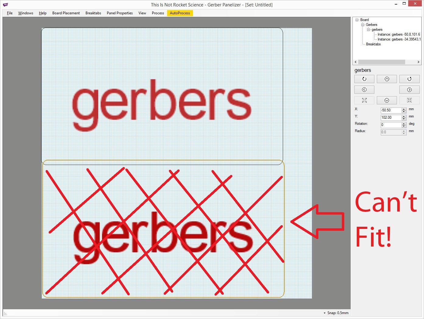
Optimization & Panelization:
There are a lot of Chinese board houses that offer steeply discounted rates on small orders of (10) 100x100mm PCBs. The goal of panelization is to maximize the amount of usable circuit boards per square inch of PCB panel. This involves optimizing layout & board shape, making provisions for individual board break-outs and the creation of edge rails. A US business card is 3.5in x 2in, or 88.9mm x 50.8mm. Only one business cards can be made within the 100x100mm space, so optimizing came down to reducing the height and reorienting footprints. The reasoning behind panelization of discounted board space is that you can produce (20) 89x51mm 2layer 0.8mm thick pcbs for 0.5665/ card shipped. The closest you could get to that rate is ordering (70) 89x51mm 2layer 0.8mm thick pcbs at 0.5275/card shipped.
IMPORTANT NOTE: Panelization for cost reduction is only fruitful for small batch orders of 10pc 100x100mm HASL lead plated pcbs. HASL should not be used as a plating for business cards as lead is toxic if ingested. In addition, there is no cost reduction possible for panelization at larger quantities, as you will just get charged by square inch. ENIG and lead free platings are not available on discounted 100x100mm board orders. Use this panelization procedure for making personal pcb projects and trinkets around your lab, not business cards. This panelization guide will continue assuming you are making a gadget about 89x51mm.
Maximum height of each card will depend on how they are broken out from the PCB panel. A lot of PCB manufacturers fabricate individual pcbs on large panels, such as 12x18in, 18x24in or 21x29in sized panels. These panels can be sub-divided into smaller sub-panels or, depending on the job size, just patterned completely in one design.
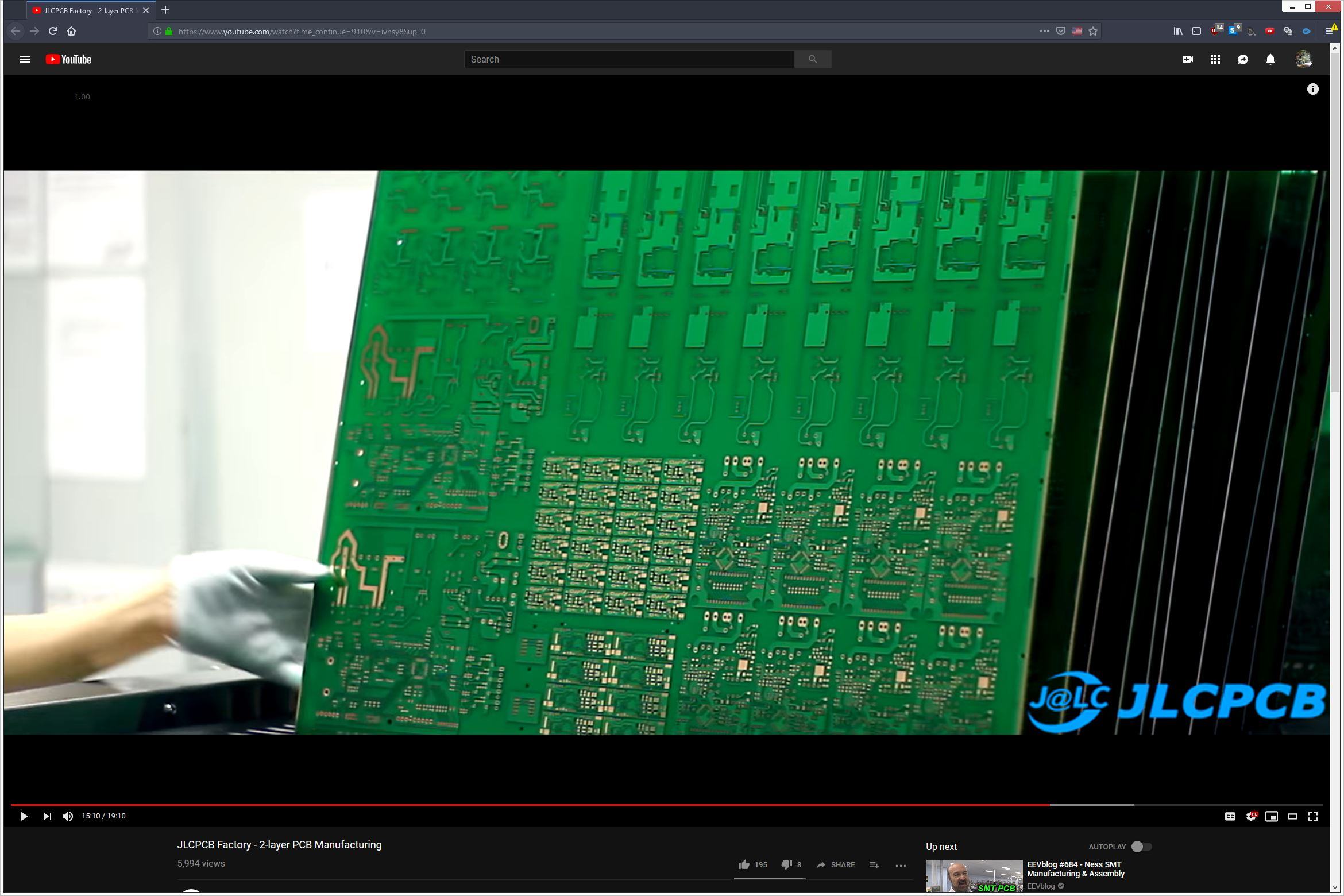
In the case of the 100x100mm board size, I believe that a bunch of chinese PCB fabricators came to the conclusion that ~100mm sq size is an ideal size to pattern on their large standardized panels, and gives them flexibility in manufacture, as long as they handle the panelization. This is a snapshot from a recent JLCPCB manufacturing video where you can clearly see that different designs are just pattern-ized on the same PCB panel and then broken out.
There are two main options for removing the individual boards from a panel - routing or V-cut. Routing involves using an endmill to route out a specific path around a circuit design. For routing to work in a panel, each individual design must be separated by 2mm, for adequate space for the endmill.
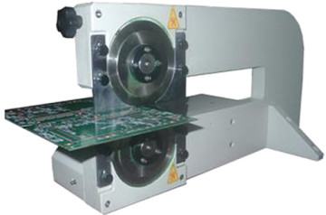
The V-cut method involves a "PCB Depaneling machine" that uses a pair of collinear mounted pizza cutter style blades to make a groove in the fiberglass circuit board. With V-cutting, direct overlapping of the edgecut or outline layer is necessary - saving board space. V-cut or v-groove is traditionally a continuous process where a cut will extend from one side of the board to the other. Sometimes a board house will allow for interrupted V-cutting but this is not always the case and it generally frowned upon.
There is a new method for pcb separation involving lasers that looks promising. This involves the use of a high power UV laser to cut directly through the fr4 material. I can imagine that massive amounts of air filtration is needed to ensure a safe working environment, but it is definitely an interesting application. Z-axis has a very encompassing video about different depaneling methods which is well worth the watch.
The benefit for v-cutting is that the spacing from cutting edge to nearest trace is less than routing. For one board house, they specify 0.4mm from edge to trace. This means I can get away with a 0.8mm gap between business cards, instead of 2mm with routing. There is a ±0.5mm tolerance for V-scoring and ±0.2mm for CNC routing from that same manufacture, but V-scoring still takes the cake.
Be mindful that each pcb fabricator is different and has different capabilities, panelization methods and tolerances. Here are direct links to the tolerances and specifics of a few pcb fabricators: PCBway, JLCPCB, Seeed/Fusion, Elecrow and Advanced Circuits. Another important note: not every PCB vendor will allow panelization at the discounted 100x100mm price bracket. Worst case scenario is you get charged a panelization fee. Some folks on eevblog have had success, so it's worth a shot. Keep the same design when panelizing this 100x100mm space as it is more common for PCB vendors to charge an extra fee if they see different circuit designs within the same sub-panel. That means any change in a gerber file counts as a different design, even if it's just a silkscreen change.
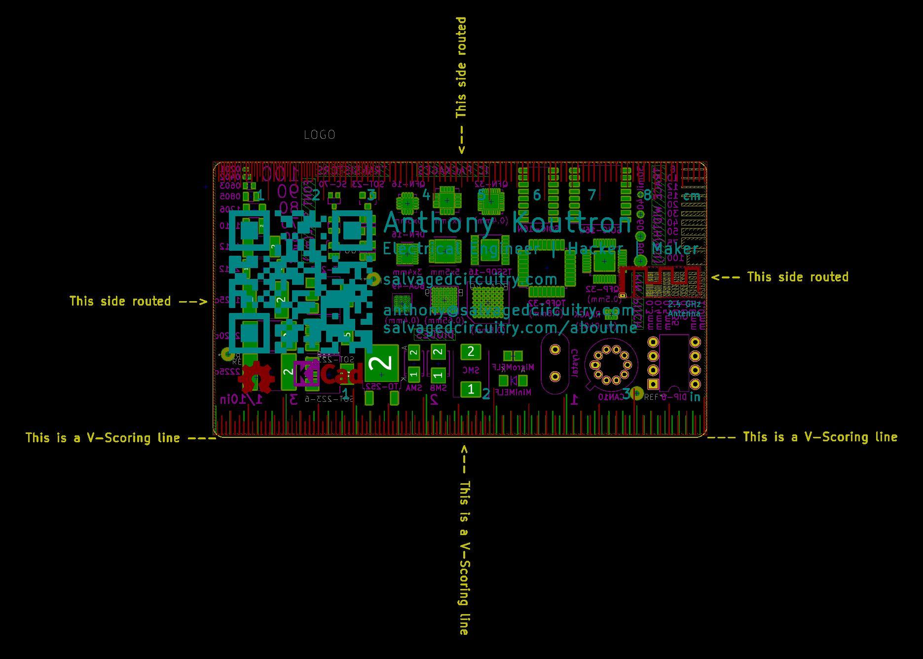
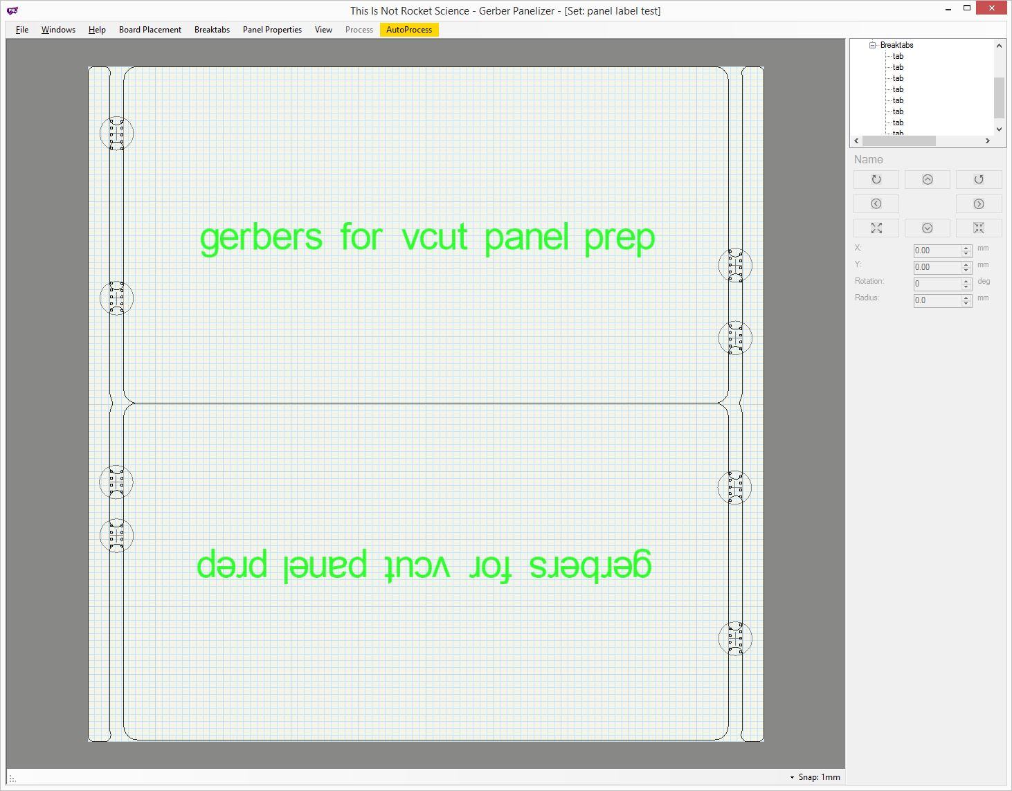
My panelized business cards use a combination of routing and grooving. V-grooving is used horizontally between the business cards and routing is used on the outer edges, sides and corners. Whatever process used to break out the individual boards, it must be indicated to the PCB manufacturer. PCBway mentioned to leave note of a v-groove in the board outline layer. I simply labeled all the processes in a spare layer like "This is a v-groove line."
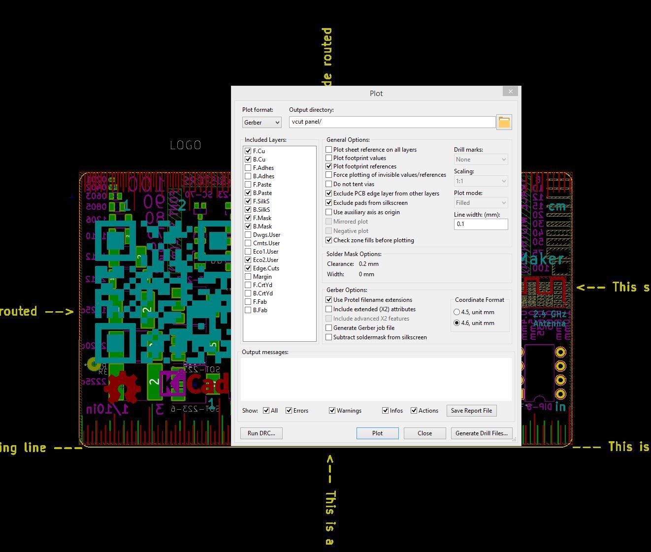
With the cutting annotated, you're ready to plot gerbers. In kicad, select "plot." The plot icon looks like a large poster printer. My plot settings and selected layers are in the attached photo. Important notes: make sure to check "use protel filename extensions" or gerber panelizer will not read your gerber files right. Hit plot. A popup should come up. Make sure to say yes to "do you want to use a path relative to..." so the path works for other people, if you plan on sharing your designs.
For generating drill files, hit the button on the lower right of the plot window. Make sure to check "merge PTH and NPTH holes into one file." Select generate drill file. This will create one edgecuts.gm1 file for the drill file instead of 2 drill files which is standard in kicad. In order for gerber panelizer to read your gerbers, change the .gm1 extension to .gko in the directory for your output gerbers. Gerber panelizer should now happily read your kicad gerbers.
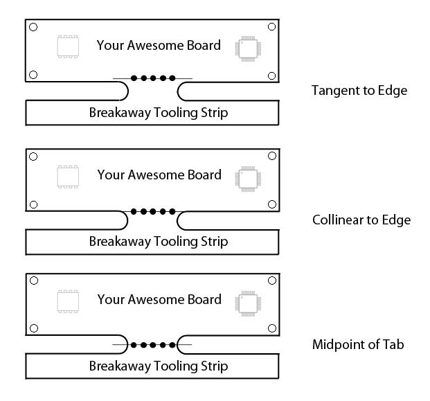
Traditionally, tabs are necessary for routing so the individual pcbs don't break away from the sub-panel. Tabs can be solid or feature tiny holes called mousebites. The location of mousebites can vary, but they are generally located tangent or collinear to the edge of the PCB. Tabs leave behind a flush but rough patch on part of a pcb edge, which has a smaller chance of cutting the person handling the boards since it does not protrude form the board.
I don't want any rough geometry which would distract from the usefulness of the business card. Thus, the best type of support tabs to use would feature mouse bites in the middle of the tab so the excess can be sanded off flush later. This adds additional processing to the cards, but it's well worth the trip to the granite sanding block.
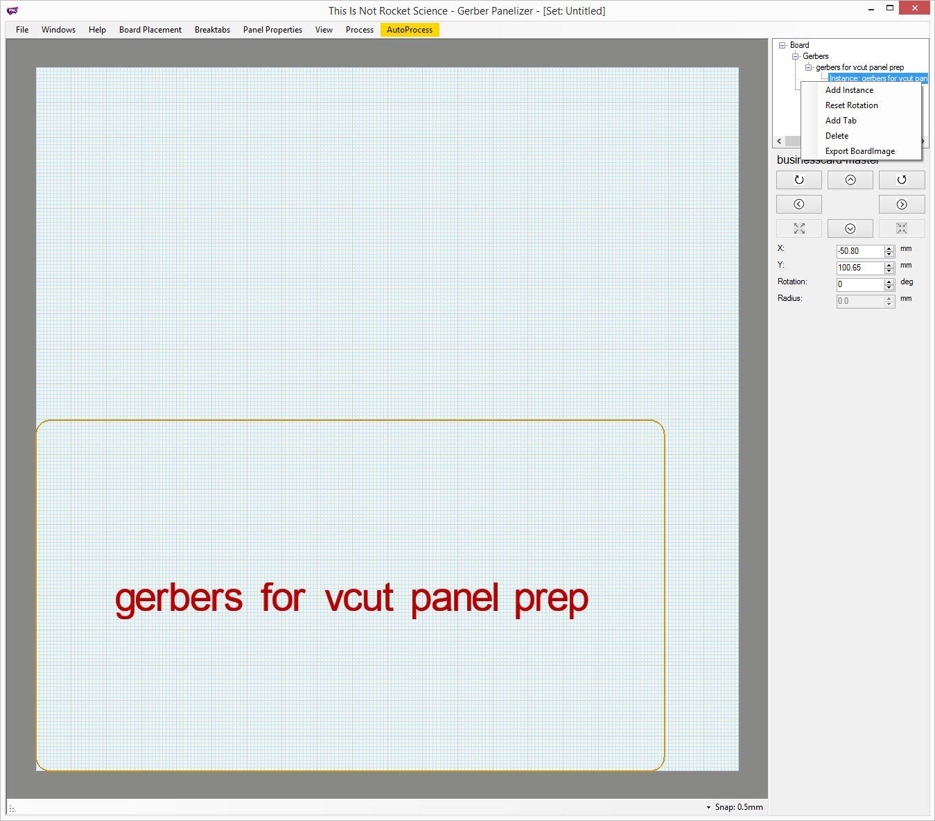
In order to pass off 2 businesscards as one PCB, you have to iterate the businesscard gerber files and merge them into one entity. To handle the creation of merged gerber files, I used "Gerber Panelizer" a free program which aids in panelizing and patternizing designs from pcb software such as eagle and Kicad. Shout out to tinkermind for suggesting elecrow and gerber panelizer.
Here's some guidelines for making patternized gerbers with gerber panelizer. Create a zip file of your output gerbers and output drill file. Open GerberPanelizer and drag in your gerber zip file. The Gerbers should be read and the edgecuts outline should show up. On the bottom right of window set snap to 0.5mm. This will make placement of the individual designs easier to line up. In the menu, go to panel properties > set width and height to 100mm. Go to top right directory tree and right click "instance." Select add instance. This creates your second design. Rotate the second design using the buttons on right. Your board may go outside viewing area while doing this. Go to view > scale 1:1 to get i back int view. For V-groove make sure to line up the boards to the orientation of v-groove. Finally, center the boards by hand or by coordinate system. File > export merged gerbers and you're ready to send out your design to a board house!
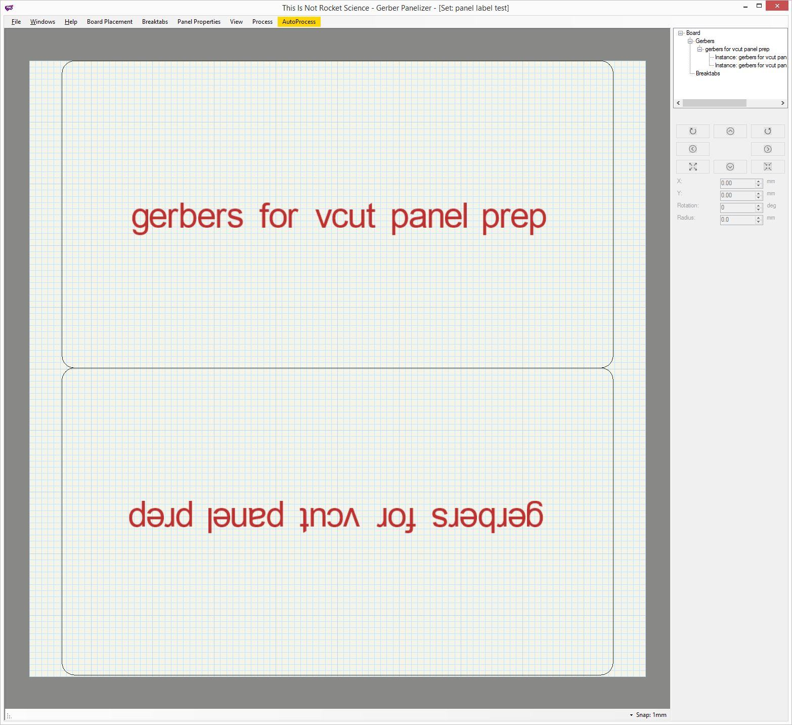
When merging the gerber files, make sure to line up the gerber files so the same edge is being v-cut for both boards. In this image you can see the gerbers rotated 180 degrees from one another. You would not want the bottom of one card to be routed while the bottom of the other is v-cut. The difference in edge finish would be quite apparent.
You will notice that I did not use edge rails for the finalized merged gerber files. This is simply because the chinese board manufacturers do not individually panelize the discounted designs. They just patternize them onto one board and break them out, as shown in the pcb manufacturing videos above. If I added edge rails, the pcb vendor would clearly pick up that I was trying to panelize within their panel and they may tack on extra fees.
So far, Gerber Panelizer has been very useful, as there is no other KiCAD panelizer option available. It also features automatic edge rail / tooling strip creation for designs, which is super handy. There are some major problems though. For one, gerbers from Kicad wont be read unless you change the file extension on the edgecuts layer from .gm1 to .gko. That was a huge annoyance that took me a while to solve. Also, the current Gerber Panelizer version has a problem where break tabs will not form between boards or between boards and the edge rail, making the creation of panels impossible. Luckily, Arsenijs on Hackaday.io made a fix so break tabs work again. Unfortunately, the toggling of mouse bits on the break tabs is not present in the fixed version and would require an entire decompiling of the original program and the fixed version, running a diff, applying the fix to the latest original version and repackaging the files back into a working program. Thanks a ton though to the original developer as it would have taken infinitely more time to manually redraw the gerbers into a merged file.
Mistakes Made Along The Way:
- Originally, in Kicad 4.06, I could not figure out how to duplicate a copper layer onto a soldermask layer. For the Kicad logo, I wanted the "Ki" text to be in the soldermask color, but the square logo outline to be exposed. The "Cad" portion be in the native soldermask color and outlined with soldermask pullback. My solution was to superimpose available kicad logo footprints that had portions of soldermask pullback on top of other variations that didn't have soldermask pull back. The correct solution was to simply open up the kicad footprint file, click a part of the logo and select which layer that geometry should be on. My results somehow came out great, but my original approach was completely absurd.
- Early on, While experimenting with custom kicad footprints, I spent a lot of time making designs in CAD or Inkscape, saving as a bitmap, then importing with the bitmap-to-component converter. I could have just exported my design to dxf and imported directly into a new footprint in Kicad instead.
- I should have spent far less time with Inkscape and just went straight to Illustrator. I would often fire up my CAD package to draw a vector shape, export it, then convert it into a bitmap just so I could avoid using Inkscape. This was before dxf import in Kicad 5.0. Inkscape is a great open source program, but it needs some serious UI/UX work to make it more user friendly.
- I Should have switched to Kicad 5.0 earlier. I waited about a month to switch and honestly, I could have been far more productive that month with 5.0.
- I did not notice the ST Micro eDesign Antenna simulator on their website when designing the NFC coil for my second PCB business card revision. The NFC coil I implemented on my first production run would have been a lot closer to NFC specification (2.35uH or 2.75uH).
- One of the challenges faced with this design was under estimating the amount of light fall off from two layers of soldermask. I originally implemented a 400mcd reverse mount led to illuminate my logo on the top side. This was a farcry from the light output actually needed. I soldered in a high powered led and a tiny ml-421 lithium battery as a quick fix.
Potential Future Additions:
- A redesign of the coil closer to 2.75uh or 2.35uh as well as a reshuffling of components on the back side of the coil should improve coil performance and allow for greater harvesting capabilities of the NFC chip. I may remove a layer of soldermask underneath the LED to improve performance as well.
- Optimize the NFC coil with a Vector Network Analyzer. This way I can appropriately measure the impact of the interfering nearby copper pads on the opposing size and maximize the coil performance.
- Leave alternative traces to an SMT coil cell battery footprint in case new coil still can't harness enough power to run a high power LED. May have to remove one side of the soldermask regardless, but that might make the card look a bit hazy around the LED footprint.
- Differential pairs and trace matching in the copper layer connected to a mid-sized FPGA footprint would look pretty sweet. Personal contact information on the silk screen would hover over a dense and busy design, but the soldermask would cover it for a very subdued effect. This image was borrowed from Tesla500.

If you're still reading this far down, thanks for following along! You deserve a massive pat on the back. Comment down below if you want to see me optimize this business card coil with a Vector Network Analyzer. Don't let me down, I need an excuse to snag an old VNA off ebay :D
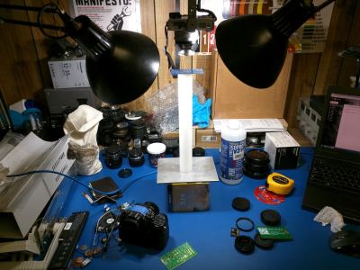
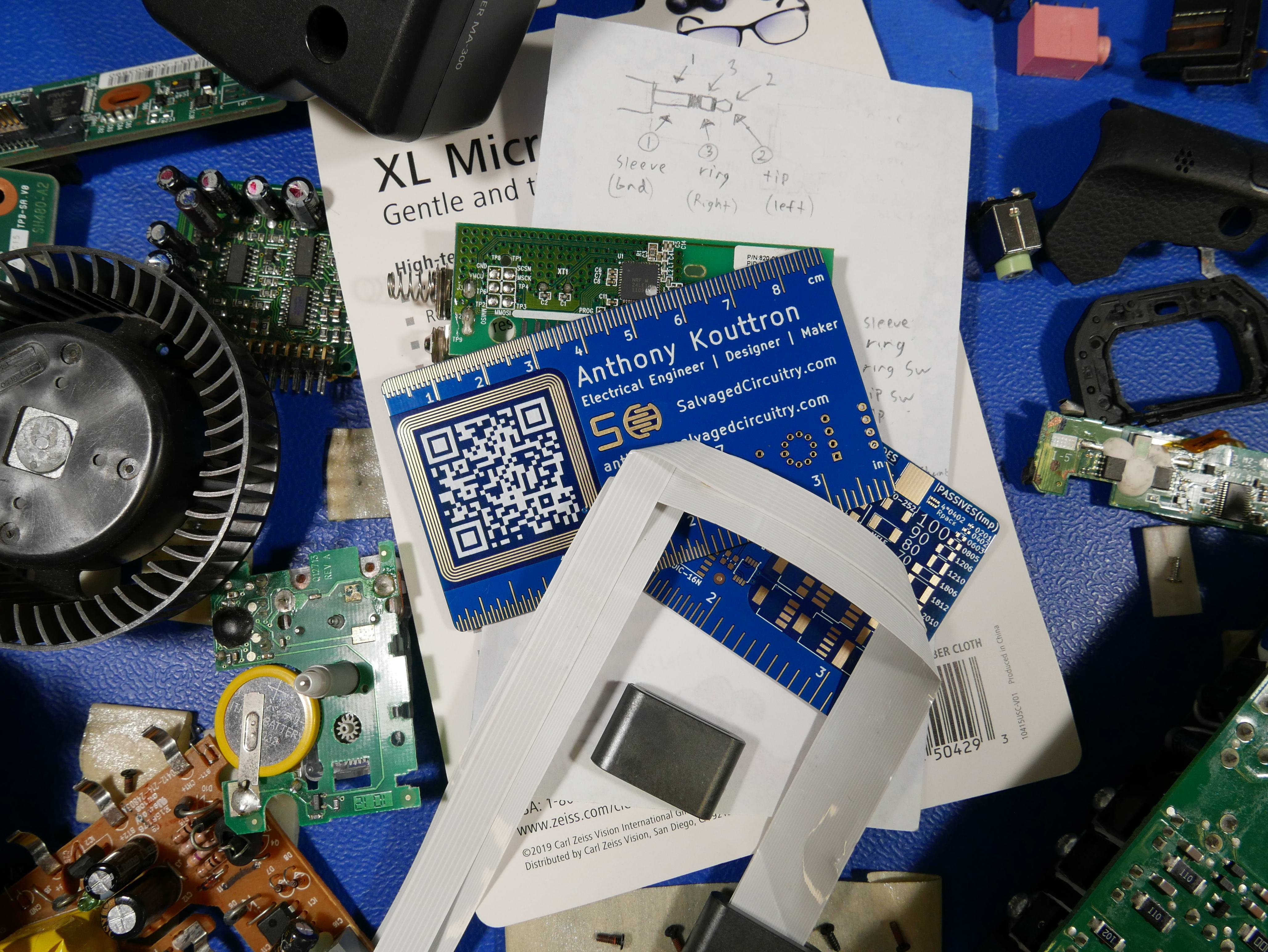
Want more? Here's a behind the scenes look at my workspace and some of the images that did not make the cut to be included in the write-up: